- 您现在的位置:买卖IC网 > PDF目录10676 > LTC1404CS8#PBF (Linear Technology)IC A/D CONV 12BIT W/SHTDN 8-SOIC PDF资料下载
参数资料
| 型号: | LTC1404CS8#PBF |
| 厂商: | Linear Technology |
| 文件页数: | 19/24页 |
| 文件大小: | 0K |
| 描述: | IC A/D CONV 12BIT W/SHTDN 8-SOIC |
| 标准包装: | 100 |
| 位数: | 12 |
| 采样率(每秒): | 600k |
| 数据接口: | MICROWIRE?,串行,SPI? |
| 转换器数目: | 1 |
| 功率耗散(最大): | 160mW |
| 电压电源: | 双 ± |
| 工作温度: | 0°C ~ 70°C |
| 安装类型: | 表面贴装 |
| 封装/外壳: | 8-SOIC(0.154",3.90mm 宽) |
| 供应商设备封装: | 8-SOIC |
| 包装: | 管件 |
| 输入数目和类型: | 1 个单端,单极;1 个单端,双极 |
| 产品目录页面: | 1346 (CN2011-ZH PDF) |
4
LTC1404
1404fa
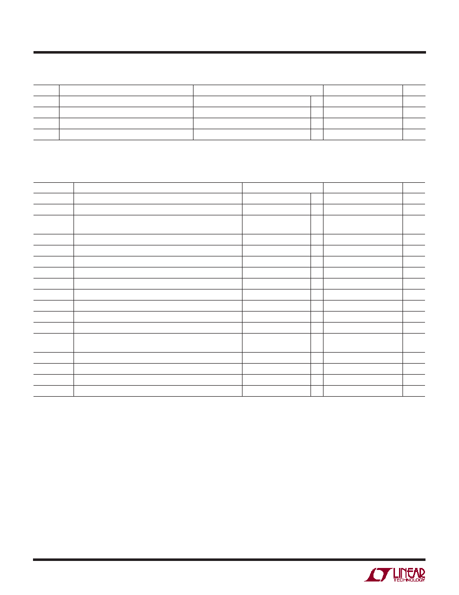
DIGITAL I PUTS AND OUTPUTS
U
SYMBOL
PARAMETER
CONDITIONS
MIN
TYP
MAX
UNITS
IOZ
Hi-Z Output Leakage DOUT
VOUT = 0V to VCC
●
±10
A
COZ
Hi-Z Output Capacitance DOUT
15
pF
ISOURCE
Output Source Current
VOUT = 0V
– 10
mA
ISINK
Output Sink Current
VOUT = VCC
10
mA
TI I G CHARACTERISTICS
W U
Note 1: Stresses beyond those listed under Absolute Maximum Ratings
may cause permanent damage to the device. Exposure to any Absolute
Maximum Rating condition for extended periods may affect device
reliability and lifetime.
Note 2: All voltage values are with respect to GND.
Note 3: When these pin voltages are taken below VSS (ground for unipolar
mode) or above VCC, they will be clamped by internal diodes. This product
can handle input currents greater than 60mA without latch-up if the pin is
driven below VSS (ground for unipolar mode) or above VCC.
Note 4: When these pin voltages are taken below VSS (ground for unipolar
mode), they will be clamped by internal diodes. This product can handle
input currents greater than 60mA without latch-up if the pin is driven
below VSS (ground for unipolar mode). These pins are not clamped to VCC.
Note 5: Guaranteed by design, not subject to test.
Note 6: Linearity, offset and full-scale specifications apply for unipolar and
bipolar modes.
Note 7: Integral nonlinearity is defined as the deviation of a code from a
straight line passing through the actual endpoints of the transfer curve.
The deviation is measured from the center of the quantization band.
Note 8: Bipolar offset is the offset voltage measured from – 0.5LSB when
the output code flickers between 0000 0000 0000 and 1111 1111 1111.
Note 9: The rising edge of CONV starts a conversion. If CONV returns low
at a bit decision point during the conversion, it can create small errors. For
best performance, ensure that CONV returns low either within 100ns after
the conversion starts (i.e., before the first bit decision) or after the 14
clock cycles. (Figure 13 Timing Diagram).
Note 10: If this timing specification is not met, the device may not respond
to a request for a conversion. To recover from this condition a NAP
request is required.
SYMBOL
PARAMETER
CONDITIONS
MIN
TYP
MAX
UNITS
fSAMPLE(MAX)
Maximum Sampling Frequency
●
600
kHz
tCONV
Conversion Time
fCLK = 9.6MHz
1.36
s
tACQ
Acquisition Time (Unipolar Mode)
200
ns
(Bipolar Mode VSS = – 5V)
160
ns
fCLK
CLK Frequency
●
0.1
9.6
MHz
tCLK
CLK Pulse Width
(Notes 5 and 10)
●
40
ns
tWK(NAP)
Time to Wake Up from Nap Mode
350
ns
t1
CLK Pulse Width to Return to Active Mode
●
40
ns
t2
CONV
↑ to CLK↑Setup Time
●
70
ns
t3
CONV
↑After Leading CLK↑
●
0ns
t4
CONV Pulse Width
(Note 9)
●
40
ns
t5
Time from CLK
↑to Sample Mode
60
ns
t6
Aperture Delay of Sample-and-Hold
Jitter < 50ps
40
ns
t7
Minimum Delay Between Conversion (Unipolar Mode)
(Note 5)
●
220
310
ns
(Bipolar Mode VSS = – 5V)
●
180
300
ns
t8
Delay Time, CLK
↑ to DOUT Valid
CLOAD = 20pF
●
40
70
ns
t9
Delay Time, CLK
↑to DOUT Hi-Z
CLOAD = 20pF
●
40
70
ns
t10
Time from Previous Data Remains Valid After CLK
↑
CLOAD = 20pF
●
10
30
ns
t11
Minimum Time Between Nap/Sleep Request to Wake Up Request (Notes 5 and 10)
●
50
ns
The
● denotes specifications which apply over the full operating temperature
range, unless otherwise noted specifications are at TA = 25°C. VCC = 5V, fSAMPLE = 600kHz, tr = tf = 5ns, unless otherwise specified.
The
● denotes specifications which apply over the full operating temperature range,
unless otherwise noted specifications are at TA = 25°C. VCC = 5V, fSAMPLE = 600kHz, tr = tf = 5ns, unless otherwise specified. See Figures
12, 13, 14.
相关PDF资料 |
PDF描述 |
|---|---|
| VI-2TP-IX-B1 | CONVERTER MOD DC/DC 13.8V 75W |
| AS1973-T | IC COMPARATOR DUAL O-D 8-MSOP |
| VI-JWH-MY-F3 | CONVERTER MOD DC/DC 52V 50W |
| AD7793BRUZ | IC ADC 24BIT SIG-DEL 3CH 16TSSOP |
| VI-BWF-MY-B1 | CONVERTER MOD DC/DC 72V 50W |
相关代理商/技术参数 |
参数描述 |
|---|---|
| LTC1404IS8 | 功能描述:IC A/D CONV 12BIT W/SHTDN 8-SOIC RoHS:否 类别:集成电路 (IC) >> 数据采集 - 模数转换器 系列:- 标准包装:1,000 系列:- 位数:16 采样率(每秒):45k 数据接口:串行 转换器数目:2 功率耗散(最大):315mW 电压电源:模拟和数字 工作温度:0°C ~ 70°C 安装类型:表面贴装 封装/外壳:28-SOIC(0.295",7.50mm 宽) 供应商设备封装:28-SOIC W 包装:带卷 (TR) 输入数目和类型:2 个单端,单极 |
| LTC1404IS8#PBF | 功能描述:IC A/D CONV 12BIT W/SHTDN 8-SOIC RoHS:是 类别:集成电路 (IC) >> 数据采集 - 模数转换器 系列:- 标准包装:1,000 系列:- 位数:16 采样率(每秒):45k 数据接口:串行 转换器数目:2 功率耗散(最大):315mW 电压电源:模拟和数字 工作温度:0°C ~ 70°C 安装类型:表面贴装 封装/外壳:28-SOIC(0.295",7.50mm 宽) 供应商设备封装:28-SOIC W 包装:带卷 (TR) 输入数目和类型:2 个单端,单极 |
| LTC1404IS8#TR | 功能描述:IC ADC 12BIT 600KSPS SHTDN 8SOIC RoHS:否 类别:集成电路 (IC) >> 数据采集 - 模数转换器 系列:- 标准包装:1,000 系列:- 位数:16 采样率(每秒):45k 数据接口:串行 转换器数目:2 功率耗散(最大):315mW 电压电源:模拟和数字 工作温度:0°C ~ 70°C 安装类型:表面贴装 封装/外壳:28-SOIC(0.295",7.50mm 宽) 供应商设备封装:28-SOIC W 包装:带卷 (TR) 输入数目和类型:2 个单端,单极 |
| LTC1404IS8#TRPBF | 功能描述:IC A/D CONV 12BIT W/SHTDN 8-SOIC RoHS:是 类别:集成电路 (IC) >> 数据采集 - 模数转换器 系列:- 标准包装:1,000 系列:- 位数:16 采样率(每秒):45k 数据接口:串行 转换器数目:2 功率耗散(最大):315mW 电压电源:模拟和数字 工作温度:0°C ~ 70°C 安装类型:表面贴装 封装/外壳:28-SOIC(0.295",7.50mm 宽) 供应商设备封装:28-SOIC W 包装:带卷 (TR) 输入数目和类型:2 个单端,单极 |
| LTC1405CGN | 功能描述:IC ADC 12BIT 5MSPS SAMPLE 28SSOP RoHS:否 类别:集成电路 (IC) >> 数据采集 - 模数转换器 系列:- 标准包装:1,000 系列:- 位数:16 采样率(每秒):45k 数据接口:串行 转换器数目:2 功率耗散(最大):315mW 电压电源:模拟和数字 工作温度:0°C ~ 70°C 安装类型:表面贴装 封装/外壳:28-SOIC(0.295",7.50mm 宽) 供应商设备封装:28-SOIC W 包装:带卷 (TR) 输入数目和类型:2 个单端,单极 |
发布紧急采购,3分钟左右您将得到回复。