- 您现在的位置:买卖IC网 > PDF目录10330 > LTC1406IGN#TR (Linear Technology)IC ADC 8BIT 20MSPS SAMPLE 24SSOP PDF资料下载
参数资料
| 型号: | LTC1406IGN#TR |
| 厂商: | Linear Technology |
| 文件页数: | 14/16页 |
| 文件大小: | 0K |
| 描述: | IC ADC 8BIT 20MSPS SAMPLE 24SSOP |
| 标准包装: | 2,500 |
| 位数: | 8 |
| 采样率(每秒): | 20M |
| 数据接口: | 并联 |
| 转换器数目: | 1 |
| 功率耗散(最大): | 225mW |
| 电压电源: | 模拟和数字,双 ± |
| 工作温度: | -40°C ~ 85°C |
| 安装类型: | 表面贴装 |
| 封装/外壳: | 24-SSOP(0.154",3.90mm 宽) |
| 供应商设备封装: | 24-SSOP |
| 包装: | 带卷 (TR) |
| 输入数目和类型: | 2 个单端,双极;1 个差分,双极 |
7
LTC1406
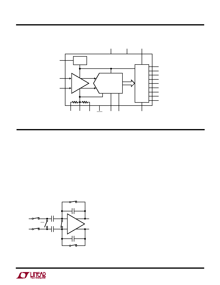
FUNCTIONAL BLOCK DIAGRA
UU
W
APPLICATIONS INFORMATION
WU
U
Conversion Details
The LTC1406 uses an internal sample-and-hold circuit and
a pipeline quantizing architecture to convert an analog
signal to an 8-bit parallel output. With CLK high the input
switches are closed and the analog input will be acquired
on the input sampling capacitors CS (see Figure 1).
On the falling edge of CLK the input switches open, captur-
ing the input signal. The sampling capacitors are then
shorted together and the charge is transferred to the hold
TRACK-AND-
HOLD AMP
DIGITAL
DATA
8-BIT
PIPELINE
ADC
2.5k
AVDD
VBIAS
VREF
OVDD
DVDD
OGND
AGND
SHDN
1.95k
2.2V
OUTPUT
DRIVERS
OF/UF
D7
D6
D5
D4
D3
D2
D1
D0
1406 BD
CLOCK
CIRCUITRY
CLK
AIN
+
7
8
94
10
3
5
6
1
23
2
11
12
22
21
20
19
18
17
16
15
24
AIN
–
DGND
–
+
CH
CLK
1406 F01
CLK
TO NEXT STAGE
CLK
AIN
+
AIN
–
CH
CS
CLK
Figure 1. Input Sample-and-Hold Amplifier
capacitors CH resulting in a differential DC voltage on the
output of the track-and-hold amplifier that is proportional
to the input signal. This differential voltage is fed into a
comparator that determines the most significant bit and
subtracts the result. The residue is then amplified by two
and passed to the next stage via a similar sample-and-hold
circuit. This continues down the eight pipeline stages. The
comparator outputs are then combined in a digital error
correction circuit. The 8-bit word is available at the output,
five clock cycles after the sampling edge.
Dynamic Performance
The LTC1406 has excellent wideband sampling capability.
The sample-and-hold amplifier has a small-signal input
bandwidth of 250MHz allowing the ADC to undersample
input signals with frequencies well beyond the converter’s
Nyquist frequency. FFT (Fast Fourier Transform) test tech-
niques are used to test the ADC’s frequency response,
distortion and noise at the rated throughput. By applying
a low distortion sine wave and analyzing the digital output
using an FFT algorithm, the ADC’s spectral content can be
examined for frequencies outside the fundamental. Figure
2 shows a typical LTC1406 FFT plot.
相关PDF资料 |
PDF描述 |
|---|---|
| MS27497E16F26S | CONN RCPT 26POS WALL MNT W/SCKT |
| AD7321BRUZ-REEL | IC ADC 12BIT+SAR 2CHAN 14-TSSOP |
| AD7265BCPZ-REEL | IC ADC 12BIT 3CHAN 1MSPS 32LFCSP |
| CS3106A-20-58P | CONN PLUG 10POS STRAIGHT W/PINS |
| AD7992BRMZ-0REEL | IC ADC 12BIT 2CHAN I2C 10MSOP |
相关代理商/技术参数 |
参数描述 |
|---|---|
| LTC1407ACMSE | 功能描述:IC ADC 14BIT 3MSPS SAMPLE 10MSOP RoHS:否 类别:集成电路 (IC) >> 数据采集 - 模数转换器 系列:- 标准包装:1,000 系列:- 位数:16 采样率(每秒):45k 数据接口:串行 转换器数目:2 功率耗散(最大):315mW 电压电源:模拟和数字 工作温度:0°C ~ 70°C 安装类型:表面贴装 封装/外壳:28-SOIC(0.295",7.50mm 宽) 供应商设备封装:28-SOIC W 包装:带卷 (TR) 输入数目和类型:2 个单端,单极 |
| LTC1407ACMSE#PBF | 功能描述:IC ADC 14BIT 3MSPS 10-MSOP RoHS:是 类别:集成电路 (IC) >> 数据采集 - 模数转换器 系列:- 标准包装:1,000 系列:- 位数:16 采样率(每秒):45k 数据接口:串行 转换器数目:2 功率耗散(最大):315mW 电压电源:模拟和数字 工作温度:0°C ~ 70°C 安装类型:表面贴装 封装/外壳:28-SOIC(0.295",7.50mm 宽) 供应商设备封装:28-SOIC W 包装:带卷 (TR) 输入数目和类型:2 个单端,单极 |
| LTC1407ACMSE#TR | 功能描述:IC ADC 14BIT 3MSPS SAMPLE 10MSOP RoHS:否 类别:集成电路 (IC) >> 数据采集 - 模数转换器 系列:- 标准包装:1,000 系列:- 位数:16 采样率(每秒):45k 数据接口:串行 转换器数目:2 功率耗散(最大):315mW 电压电源:模拟和数字 工作温度:0°C ~ 70°C 安装类型:表面贴装 封装/外壳:28-SOIC(0.295",7.50mm 宽) 供应商设备封装:28-SOIC W 包装:带卷 (TR) 输入数目和类型:2 个单端,单极 |
| LTC1407ACMSE#TRPBF | 功能描述:IC ADC 14BIT 3MSPS SAMPLE 10MSOP RoHS:是 类别:集成电路 (IC) >> 数据采集 - 模数转换器 系列:- 标准包装:1,000 系列:- 位数:16 采样率(每秒):45k 数据接口:串行 转换器数目:2 功率耗散(最大):315mW 电压电源:模拟和数字 工作温度:0°C ~ 70°C 安装类型:表面贴装 封装/外壳:28-SOIC(0.295",7.50mm 宽) 供应商设备封装:28-SOIC W 包装:带卷 (TR) 输入数目和类型:2 个单端,单极 |
| LTC1407ACMSE-1 | 功能描述:IC ADC 14BIT 3MSPS SAMPLE 10MSOP RoHS:否 类别:集成电路 (IC) >> 数据采集 - 模数转换器 系列:- 标准包装:1,000 系列:- 位数:16 采样率(每秒):45k 数据接口:串行 转换器数目:2 功率耗散(最大):315mW 电压电源:模拟和数字 工作温度:0°C ~ 70°C 安装类型:表面贴装 封装/外壳:28-SOIC(0.295",7.50mm 宽) 供应商设备封装:28-SOIC W 包装:带卷 (TR) 输入数目和类型:2 个单端,单极 |
发布紧急采购,3分钟左右您将得到回复。