- 您现在的位置:买卖IC网 > PDF目录10225 > LTC1412IG#PBF (Linear Technology)IC A/D CONV 12BIT SAMPLNG 28SSOP PDF资料下载
参数资料
| 型号: | LTC1412IG#PBF |
| 厂商: | Linear Technology |
| 文件页数: | 4/16页 |
| 文件大小: | 0K |
| 描述: | IC A/D CONV 12BIT SAMPLNG 28SSOP |
| 标准包装: | 47 |
| 位数: | 12 |
| 采样率(每秒): | 3M |
| 数据接口: | 并联 |
| 转换器数目: | 1 |
| 功率耗散(最大): | 220mW |
| 电压电源: | 双 ± |
| 工作温度: | -40°C ~ 85°C |
| 安装类型: | 表面贴装 |
| 封装/外壳: | 28-SSOP(0.209",5.30mm 宽) |
| 供应商设备封装: | 28-SSOP |
| 包装: | 管件 |
| 输入数目和类型: | 2 个单端,双极;1 个差分,双极 |
12
LTC1412
APPLICATIONS INFORMATION
WU
U
LTC1412
AIN
+
ANALOG INPUT
5V
AIN
–
VREF
REFCOMP
AGND
1412 F08b
1
2
3
4
5
10
F
VIN
VOUT
LT1019A-2.5
RIPPLE FREQUENCY (Hz)
–80
AMPLITUDE
OF
POWER
SUPPLY
FEEDTHROUGH
(dB)
–40
0
–100
–60
–20
10k
100k
1M
10M
1412 G08
–120
1k
VSS
VDD
DGND
mode voltage. THD will degrade as the inputs approach
either power supply rail, from – 86dB with a common
mode of 0V to –75dB with a common mode of 2.5V
or – 2.5V.
Full-Scale and Offset Adjustment
Figure 11a shows the ideal input/output characteristics for
the LTC1412. The code transitions occur midway between
successive integer LSB values (i.e., – FS/2 + 0.5LSB,
– FS/2 + 1.5LSB, – FS/2 + 2.5LSB,...FS/2 – 1.5LSB, FS/2 –
0.5LSB). The output is two’s complement binary with
1LSB = FS – (– FS)/4096 = 5V/4096 = 1.22mV.
Differential Inputs
The LTC1412 has a unique differential sample-and-hold
circuit that allows rail-to-rail inputs. The ADC will always
convert the difference of AIN+ – (AIN–) independent of the
common mode voltage. The common mode rejection
holds up to extremely high frequencies, see Figure 10. The
only requirement is that both inputs cannot exceed the
AVDD or AVSS power supply voltages. Integral nonlinearity
errors (INL) and differential nonlinearity errors (DNL) are
independent of the common mode voltage, however, the
bipolar zero error (BZE) will vary. The change in BZE is
typically less than 0.1% of the common mode voltage.
Dynamic performance is also affected by the common
In applications where absolute accuracy is important,
offset and full-scale errors can be adjusted to zero. Offset
error must be adjusted before full-scale error. Figure 11b
shows the extra components required for full-scale error
adjustment. Zero offset is achieved by adjusting the offset
applied to the AIN– input. For zero offset error apply
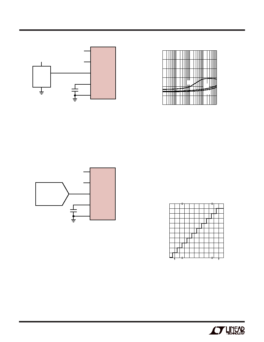
Figure 10. CMRR vs Input Frequency
Figure 8b. Using the LT1019-2.5 as an External Reference
The VREF pin can be driven with a DAC or other means
shown in Figure 9. This is useful in applications where the
peak input signal amplitude may vary. The input span of
the ADC can then be adjusted to match the peak input
signal, maximizing the signal-to-noise ratio. The filtering
of the internal LTC1412 reference amplifier will limit the
bandwidth and settling time of this circuit. A settling time
of 5ms should be allowed for after a reference adjustment.
LTC1412
AIN
+
ANALOG INPUT
1.25V TO 3V
DIFFERENTIAL
AIN
–
VREF
REFCOMP
AGND
1412 F09
1
2
3
4
5
10
F
LTC1450
1.25V TO 3V
Figure 9. Driving VREF with a DAC
INPUT VOLTAGE (V)
OUTPUT
CODE
1412 F11a
111...111
111...110
111...101
000...000
000...001
000...010
FS – 1LSB
Figure 11a. LTC1412 Transfer Characteristics
相关PDF资料 |
PDF描述 |
|---|---|
| SP491EN-L/TR | IC TXRX RS485 FULL DUPLX 14NSOIC |
| LTC1412IG | IC A/D CONV 12BIT SAMPLNG 28SSOP |
| SP490EN-L/TR | IC TXRX RS485 FULL DUPLEX 8NSOIC |
| LTC1418AIN | IC A/D CONV 14BIT SRL&PAR 28-DIP |
| SP481ECN-L/TR | IC TXRX RS484 HALF DUPLEX 8NSOIC |
相关代理商/技术参数 |
参数描述 |
|---|---|
| LTC1414CGN | 功能描述:IC A/D CONV 14BIT SAMPLNG 28SSOP RoHS:否 类别:集成电路 (IC) >> 数据采集 - 模数转换器 系列:- 标准包装:1,000 系列:- 位数:12 采样率(每秒):300k 数据接口:并联 转换器数目:1 功率耗散(最大):75mW 电压电源:单电源 工作温度:0°C ~ 70°C 安装类型:表面贴装 封装/外壳:24-SOIC(0.295",7.50mm 宽) 供应商设备封装:24-SOIC 包装:带卷 (TR) 输入数目和类型:1 个单端,单极;1 个单端,双极 |
| LTC1414CGN#PBF | 功能描述:IC A/D CONV 14BIT SAMPLNG 28SSOP RoHS:是 类别:集成电路 (IC) >> 数据采集 - 模数转换器 系列:- 标准包装:1 系列:microPOWER™ 位数:8 采样率(每秒):1M 数据接口:串行,SPI? 转换器数目:1 功率耗散(最大):- 电压电源:模拟和数字 工作温度:-40°C ~ 125°C 安装类型:表面贴装 封装/外壳:24-VFQFN 裸露焊盘 供应商设备封装:24-VQFN 裸露焊盘(4x4) 包装:Digi-Reel® 输入数目和类型:8 个单端,单极 产品目录页面:892 (CN2011-ZH PDF) 其它名称:296-25851-6 |
| LTC1414CGN#PBF | 制造商:Linear Technology 功能描述:ADC, 14BIT, 2.2MSPS, SSOP-28 |
| LTC1414CGN#TR | 功能描述:IC ADC 14BIT 2.2MSPS SMPL 28SSOP RoHS:否 类别:集成电路 (IC) >> 数据采集 - 模数转换器 系列:- 标准包装:1,000 系列:- 位数:12 采样率(每秒):300k 数据接口:并联 转换器数目:1 功率耗散(最大):75mW 电压电源:单电源 工作温度:0°C ~ 70°C 安装类型:表面贴装 封装/外壳:24-SOIC(0.295",7.50mm 宽) 供应商设备封装:24-SOIC 包装:带卷 (TR) 输入数目和类型:1 个单端,单极;1 个单端,双极 |
| LTC1414CGN#TRPBF | 功能描述:IC A/D CONV 14BIT SAMPLNG 28SSOP RoHS:是 类别:集成电路 (IC) >> 数据采集 - 模数转换器 系列:- 标准包装:1,000 系列:- 位数:12 采样率(每秒):300k 数据接口:并联 转换器数目:1 功率耗散(最大):75mW 电压电源:单电源 工作温度:0°C ~ 70°C 安装类型:表面贴装 封装/外壳:24-SOIC(0.295",7.50mm 宽) 供应商设备封装:24-SOIC 包装:带卷 (TR) 输入数目和类型:1 个单端,单极;1 个单端,双极 |
发布紧急采购,3分钟左右您将得到回复。