- 您现在的位置:买卖IC网 > PDF目录2003 > LTC1414IGN#TRPBF (Linear Technology)IC A/D CONV 14BIT SAMPLNG 28SSOP PDF资料下载
参数资料
| 型号: | LTC1414IGN#TRPBF |
| 厂商: | Linear Technology |
| 文件页数: | 10/20页 |
| 文件大小: | 0K |
| 描述: | IC A/D CONV 14BIT SAMPLNG 28SSOP |
| 标准包装: | 2,500 |
| 位数: | 14 |
| 采样率(每秒): | 2.2M |
| 数据接口: | 并联 |
| 转换器数目: | 1 |
| 功率耗散(最大): | 230mW |
| 电压电源: | 双 ± |
| 工作温度: | -40°C ~ 85°C |
| 安装类型: | 表面贴装 |
| 封装/外壳: | 28-SSOP(0.154",3.90mm 宽) |
| 供应商设备封装: | 28-SSOP |
| 包装: | 带卷 (TR) |
| 输入数目和类型: | 2 个单端,双极;1 个差分,双极 |
18
LTC1414
Digital Interface
The A/D converter has just one control input CONVST.
Data is output on 14-bit parallel bus. An additional output
BUSY indicates the converter status.
DIGITAL OUTPUTS
The parallel digital outputs of the LTC1414 are designed to
interface to TTL and CMOS logic. The output data is two’s
complement coded.
The output drivers have a separate power pin (OVDD) and
ground pin (OGND). This allows relatively noisy output
ground and the output supply bypass ground to be sepa-
rated from the other ADC grounds. Additionally, the OVDD
pin may be driven by the supply of the logic that is being
driven. For example, the OVDD supply may be 3V while
LTC1414 DVDD and AVDD pins are 5V, allowing 3V logic to
be driven directly.
Care should be taken to not load the digital outputs with
excessive capacitance. Large capacitive loads result in
large charging currents which can cause conversion er-
rors. It is recommended that the capacitive loading is kept
under 20pF. If it is not possible to keep the capacitance
low, a buffer or latch may be used to isolate the LTC1414
from the capacitive load.
Timing and Control
The conversion start is controlled by the CONVST input.
The falling edge of CONVST will start a conversion. Once
initiated, it cannot be restarted until the conversion is
complete. Converter status is indicated by the BUSY
output. BUSY is low during a conversion.
APPLICATIONS INFORMATION
WU
U
The output data is updated at the end of the conversion as
BUSY rises. Output data is updated coincident with the
rising edge of BUSY. Data will be valid, and can be latched,
20ns after the rising edge of BUSY. Valid data can also be
latched with the falling edge of BUSY or with the rising
edge of CONVST. In the latter two cases the data latched
will be for the previous conversion.
CONVST Drive Considerations
Timing jitter of the CONVST signal can adversely affect the
noise performance of the LTC1414 when the input signal
contains high slew rate components. The falling edge of
CONVST determines the sampling instant. Any uncer-
tainty in this sampling instant will translate to voltage
noise when a fast changing input signal is being sampled.
For a full amplitude sinusoidal input, the relationship
between timing jitter (tjitter) and SNRj is
SNRj = 20log(1/2π fIN tjitter)
where SNRj is the signal-to-jitter noise ratio.
The internal circuitry of the LTC1414 has been optimized
for ultralow jitter (typically 3ps RMS). The external clock
drive circuitry is equally important and must also have low
jitter to achieve low noise.
Internal Clock
The internal clock is factory trimmed to achieve a typical
conversion time of 330ns and a maximum conversion
time over the full operating temperature range of 400ns.
No external adjustments are required. The guaranteed
maximum acquisition time is 100ns. In addition, a through-
put time (acquisition + conversion) of 454ns and a mini-
mum sampling rate of 2.2Msps is guaranteed.
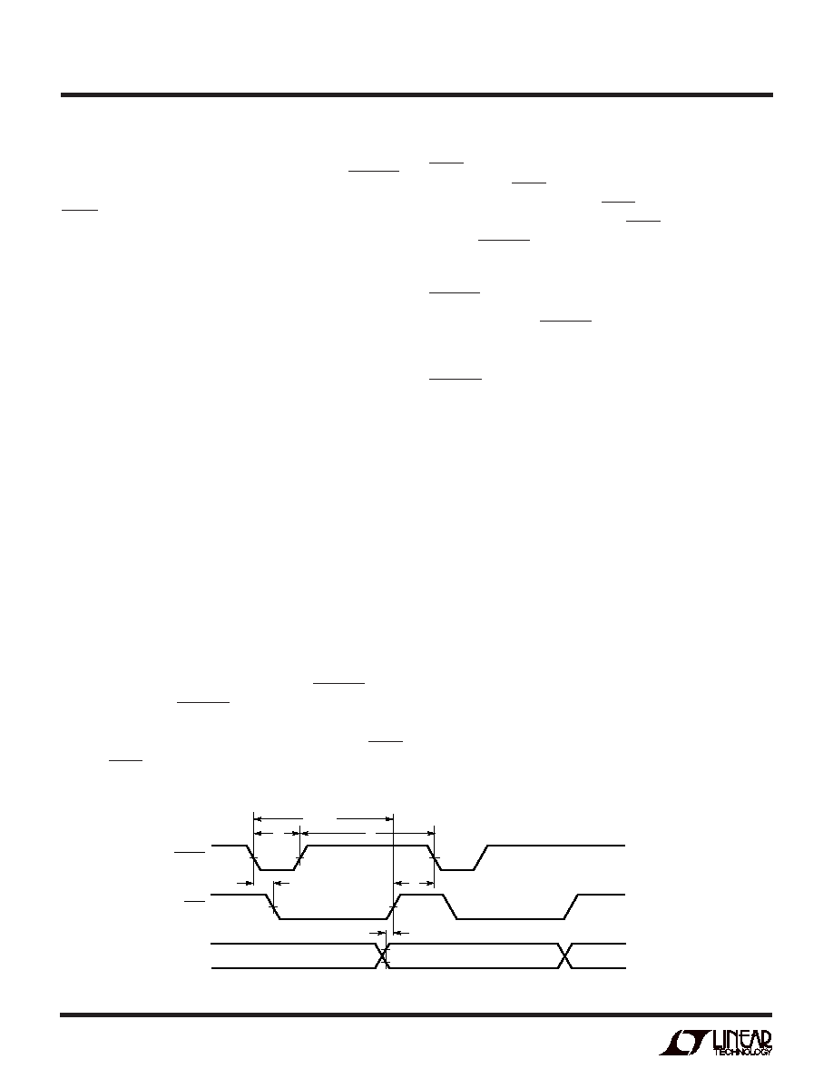
Figure 17. Timing Diagram
DATA (N – 1)
DB13 TO DB0
CONVST
BUSY
1414 F17
t4
t5
tCONV
t1
t3
t2
DATA N
DB13 TO DB0
DATA (N + 1)
DB13 TO DB0
DATA
相关PDF资料 |
PDF描述 |
|---|---|
| LTC1415CG#TRPBF | IC A/D CONV 12BIT SAMPLNG 28SSOP |
| LTC1416IG#TR | IC ADC 14BIT 400KSPS SMPL 28SSOP |
| LTC1417AIGN#TR | IC ADC 14BIT 400KSPS SMPL 16SSOP |
| LTC1418ACG#TRPBF | IC A/D CONV 14BIT SRL&PAR 28SSOP |
| LTC1419AISW#TRPBF | IC A/D CONV 14BIT SAMPLNG 28SOIC |
相关代理商/技术参数 |
参数描述 |
|---|---|
| LTC1415CG | 功能描述:IC A/D CONV 12BIT SAMPLNG 28SSOP RoHS:否 类别:集成电路 (IC) >> 数据采集 - 模数转换器 系列:- 标准包装:1,000 系列:- 位数:12 采样率(每秒):300k 数据接口:并联 转换器数目:1 功率耗散(最大):75mW 电压电源:单电源 工作温度:0°C ~ 70°C 安装类型:表面贴装 封装/外壳:24-SOIC(0.295",7.50mm 宽) 供应商设备封装:24-SOIC 包装:带卷 (TR) 输入数目和类型:1 个单端,单极;1 个单端,双极 |
| LTC1415CG#PBF | 功能描述:IC A/D CONV 12BIT SAMPLNG 28SSOP RoHS:是 类别:集成电路 (IC) >> 数据采集 - 模数转换器 系列:- 其它有关文件:TSA1204 View All Specifications 标准包装:1 系列:- 位数:12 采样率(每秒):20M 数据接口:并联 转换器数目:2 功率耗散(最大):155mW 电压电源:模拟和数字 工作温度:-40°C ~ 85°C 安装类型:表面贴装 封装/外壳:48-TQFP 供应商设备封装:48-TQFP(7x7) 包装:Digi-Reel® 输入数目和类型:4 个单端,单极;2 个差分,单极 产品目录页面:1156 (CN2011-ZH PDF) 其它名称:497-5435-6 |
| LTC1415CG#TR | 功能描述:IC ADC 12BIT 1.25MSPS SMP 28SSOP RoHS:否 类别:集成电路 (IC) >> 数据采集 - 模数转换器 系列:- 标准包装:1,000 系列:- 位数:12 采样率(每秒):300k 数据接口:并联 转换器数目:1 功率耗散(最大):75mW 电压电源:单电源 工作温度:0°C ~ 70°C 安装类型:表面贴装 封装/外壳:24-SOIC(0.295",7.50mm 宽) 供应商设备封装:24-SOIC 包装:带卷 (TR) 输入数目和类型:1 个单端,单极;1 个单端,双极 |
| LTC1415CG#TRPBF | 功能描述:IC A/D CONV 12BIT SAMPLNG 28SSOP RoHS:是 类别:集成电路 (IC) >> 数据采集 - 模数转换器 系列:- 产品培训模块:Lead (SnPb) Finish for COTS Obsolescence Mitigation Program 标准包装:2,500 系列:- 位数:12 采样率(每秒):3M 数据接口:- 转换器数目:- 功率耗散(最大):- 电压电源:- 工作温度:- 安装类型:表面贴装 封装/外壳:SOT-23-6 供应商设备封装:SOT-23-6 包装:带卷 (TR) 输入数目和类型:- |
| LTC1415CSW | 功能描述:IC A/D CONV 12BIT SAMPLNG 28SOIC RoHS:否 类别:集成电路 (IC) >> 数据采集 - 模数转换器 系列:- 标准包装:1,000 系列:- 位数:12 采样率(每秒):300k 数据接口:并联 转换器数目:1 功率耗散(最大):75mW 电压电源:单电源 工作温度:0°C ~ 70°C 安装类型:表面贴装 封装/外壳:24-SOIC(0.295",7.50mm 宽) 供应商设备封装:24-SOIC 包装:带卷 (TR) 输入数目和类型:1 个单端,单极;1 个单端,双极 |
发布紧急采购,3分钟左右您将得到回复。