- 您现在的位置:买卖IC网 > PDF目录10533 > LTC1415CG#PBF (Linear Technology)IC A/D CONV 12BIT SAMPLNG 28SSOP PDF资料下载
参数资料
| 型号: | LTC1415CG#PBF |
| 厂商: | Linear Technology |
| 文件页数: | 11/24页 |
| 文件大小: | 0K |
| 描述: | IC A/D CONV 12BIT SAMPLNG 28SSOP |
| 标准包装: | 47 |
| 位数: | 12 |
| 采样率(每秒): | 1.25M |
| 数据接口: | 并联 |
| 转换器数目: | 1 |
| 功率耗散(最大): | 100mW |
| 电压电源: | 单电源 |
| 工作温度: | 0°C ~ 70°C |
| 安装类型: | 表面贴装 |
| 封装/外壳: | 28-SSOP(0.209",5.30mm 宽) |
| 供应商设备封装: | 28-SSOP |
| 包装: | 管件 |
| 输入数目和类型: | 2 个单端,双极;1 个差分,双极 |
19
LTC1415
U
S
A
O
PPLICATI
WU
U
I FOR ATIO
In slow memory and ROM modes (Figures 19 and 20) CS
is tied low and CONVST and RD are tied together. The MPU
starts the conversion and reads the output with the RD
signal. Conversions are started by the MPU or DSP (no
external sample clock).
In slow memory mode the processor applies a logic low to
RD (= CONVST), starting the conversion. BUSY goes low,
forcing the processor into a WAIT state. The previous
conversion result appears on the data outputs. When the
conversion is complete, the new conversion results ap-
pear on the data outputs; BUSY goes high, releasing the
processor and the processor takes RD (= CONVST) back
high and reads the new conversion data.
In ROM mode, the processor takes RD (= CONVST) low,
starting a conversion and reading the previous conversion
result. After the conversion is complete, the processor can
read the new result and initiate another conversion.
t4
SHDN
CONVST
1415 F14b
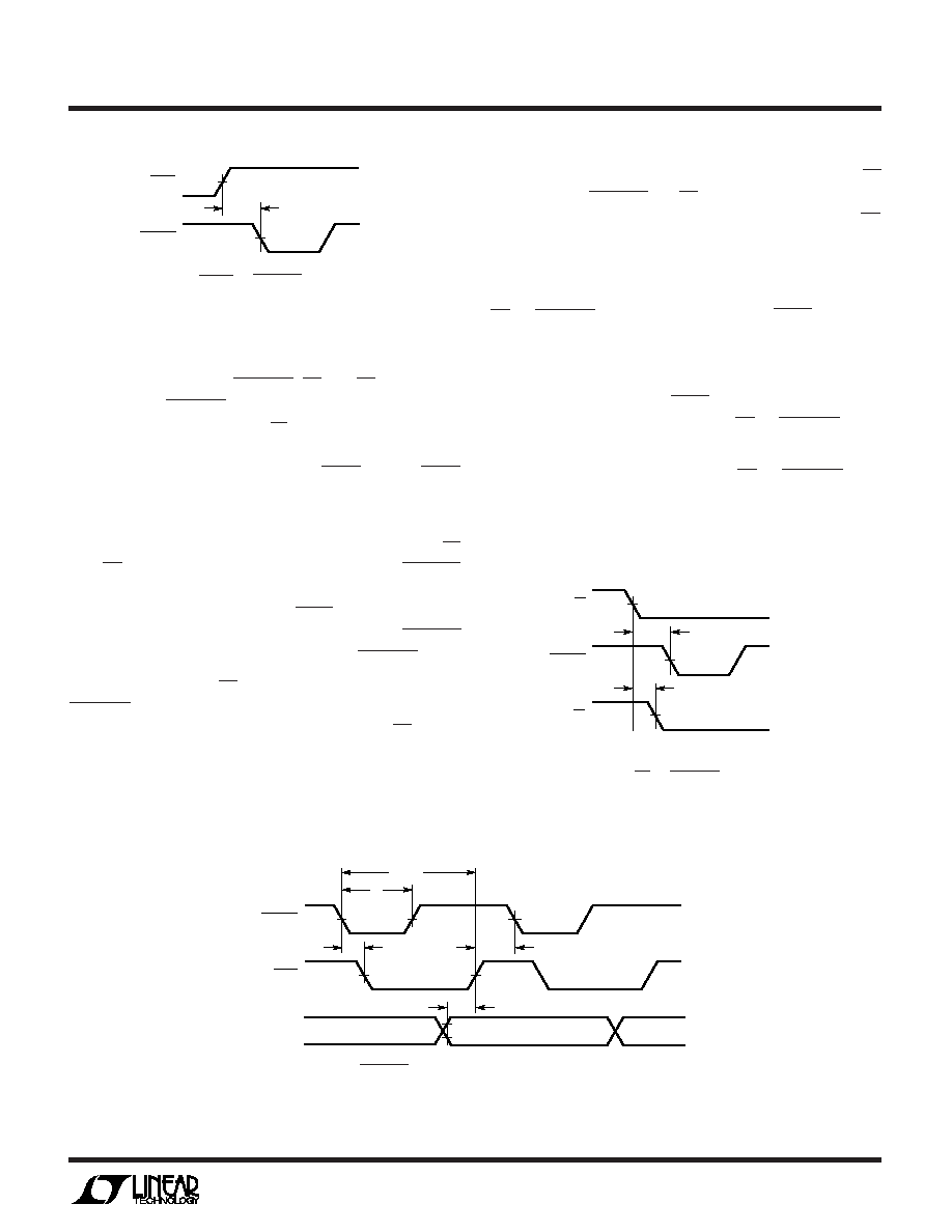
Figure 14b. SHDN to CONVST Wake-Up Timing
Timing and Control
Conversion start and data read operations are controlled
by three digital inputs: CONVST, CS and RD. A logic “0”
applied to the CONVST pin will start a conversion after the
ADC has been selected (i.e., CS is low). Once initiated, it
cannot be restarted until the conversion is complete.
Converter status is indicated by the BUSY output. BUSY
is low during a conversion.
Figures 16 through 20 show several different modes of
operation. In modes 1a and 1b (Figures 16 and 18) CS
and RD are both tied low. The falling edge of CONVST
starts the conversion. The data outputs are always enabled
and data can be latched with the BUSY rising edge. Mode
1a shows operation with a narrow logic low CONVST
pulse. Mode 1b shows a narrow logic high CONVST pulse.
In mode 2 (Figure 18) CS is tied low. The falling edge of the
CONVST signal again starts the conversion. Data outputs
are in three-state until read by the MPU with the RD signal.
Mode 2 can be used for operation with a shared MPU
databus.
Figure 15. CS to CONVST Setup Timing
t2
t1
CS
CONVST
RD
1415 F15
DATA (N – 1)
DB11 TO DB0
CONVST
BUSY
1415 F16
t5
tCONV
t6
t8
t7
DATA N
DB11 TO DB0
DATA (N + 1)
DB11 TO DB0
DATA
Figure 16. Mode 1a CONVST Starts a Conversion. Data Outputs Always Enabled
相关PDF资料 |
PDF描述 |
|---|---|
| AMIS30660CANH2G | TRANSCEIVER CAN HS 5V 8-SOIC |
| VE-J3Y-MY-F2 | CONVERTER MOD DC/DC 3.3V 33W |
| MS3101A18-13P | CONN RCPT 4POS FREE HNG W/PINS |
| AD7862ANZ-10 | IC ADC 12BIT DUAL 250KSPS 28DIP |
| MS3101A16S-4P | CONN RCPT 2POS FREE HNG W/PINS |
相关代理商/技术参数 |
参数描述 |
|---|---|
| LTC1415CSW | 功能描述:IC A/D CONV 12BIT SAMPLNG 28SOIC RoHS:否 类别:集成电路 (IC) >> 数据采集 - 模数转换器 系列:- 标准包装:1,000 系列:- 位数:12 采样率(每秒):300k 数据接口:并联 转换器数目:1 功率耗散(最大):75mW 电压电源:单电源 工作温度:0°C ~ 70°C 安装类型:表面贴装 封装/外壳:24-SOIC(0.295",7.50mm 宽) 供应商设备封装:24-SOIC 包装:带卷 (TR) 输入数目和类型:1 个单端,单极;1 个单端,双极 |
| LTC1415CSW#PBF | 功能描述:IC A/D CONV 12BIT SAMPLNG 28SOIC RoHS:是 类别:集成电路 (IC) >> 数据采集 - 模数转换器 系列:- 标准包装:1 系列:microPOWER™ 位数:8 采样率(每秒):1M 数据接口:串行,SPI? 转换器数目:1 功率耗散(最大):- 电压电源:模拟和数字 工作温度:-40°C ~ 125°C 安装类型:表面贴装 封装/外壳:24-VFQFN 裸露焊盘 供应商设备封装:24-VQFN 裸露焊盘(4x4) 包装:Digi-Reel® 输入数目和类型:8 个单端,单极 产品目录页面:892 (CN2011-ZH PDF) 其它名称:296-25851-6 |
| LTC1415CSW#TR | 功能描述:IC ADC 12BIT 1.25MSPS SMP 28SOIC RoHS:否 类别:集成电路 (IC) >> 数据采集 - 模数转换器 系列:- 标准包装:1,000 系列:- 位数:12 采样率(每秒):300k 数据接口:并联 转换器数目:1 功率耗散(最大):75mW 电压电源:单电源 工作温度:0°C ~ 70°C 安装类型:表面贴装 封装/外壳:24-SOIC(0.295",7.50mm 宽) 供应商设备封装:24-SOIC 包装:带卷 (TR) 输入数目和类型:1 个单端,单极;1 个单端,双极 |
| LTC1415CSW#TRPBF | 功能描述:IC A/D CONV 12BIT SAMPLNG 28SOIC RoHS:是 类别:集成电路 (IC) >> 数据采集 - 模数转换器 系列:- 标准包装:1,000 系列:- 位数:12 采样率(每秒):300k 数据接口:并联 转换器数目:1 功率耗散(最大):75mW 电压电源:单电源 工作温度:0°C ~ 70°C 安装类型:表面贴装 封装/外壳:24-SOIC(0.295",7.50mm 宽) 供应商设备封装:24-SOIC 包装:带卷 (TR) 输入数目和类型:1 个单端,单极;1 个单端,双极 |
| LTC1415CSWPBF | 制造商:Linear Technology 功能描述:LTC1415CSWPBF |
发布紧急采购,3分钟左右您将得到回复。