- 您现在的位置:买卖IC网 > PDF目录10533 > LTC1415CG#PBF (Linear Technology)IC A/D CONV 12BIT SAMPLNG 28SSOP PDF资料下载
参数资料
| 型号: | LTC1415CG#PBF |
| 厂商: | Linear Technology |
| 文件页数: | 2/24页 |
| 文件大小: | 0K |
| 描述: | IC A/D CONV 12BIT SAMPLNG 28SSOP |
| 标准包装: | 47 |
| 位数: | 12 |
| 采样率(每秒): | 1.25M |
| 数据接口: | 并联 |
| 转换器数目: | 1 |
| 功率耗散(最大): | 100mW |
| 电压电源: | 单电源 |
| 工作温度: | 0°C ~ 70°C |
| 安装类型: | 表面贴装 |
| 封装/外壳: | 28-SSOP(0.209",5.30mm 宽) |
| 供应商设备封装: | 28-SSOP |
| 包装: | 管件 |
| 输入数目和类型: | 2 个单端,双极;1 个差分,双极 |
10
LTC1415
the presence of another sinusoidal input at a different
frequency.
If two pure sine waves of frequencies fa and fb are applied
to the ADC input, nonlinearities in the ADC transfer func-
tion can create distortion products at the sum and differ-
ence frequencies of mfa + – nfb, where m and n = 0, 1, 2,
3, etc. For example, the 2nd order IMD terms include
(fa + fb). If the two input sine waves are equal in magni-
tude, the value (in decibels) of the 2nd order IMD products
can be expressed by the following formula:
IMD fa
fb
Log
+
() = 20
Amplitude at (fa + fb)
Amplitude at fa
Peak Harmonic or Spurious Noise
The peak harmonic or spurious noise is the largest spec-
tral component excluding the input signal and DC. This
value is expressed in decibels relative to the RMS value of
a full-scale input signal.
Full-Power and Full-Linear Bandwidth
The full-power bandwidth is that input frequency at which
the amplitude of the reconstructed fundamental is
reduced by 3dB for a full-scale input signal.
The full-linear bandwidth is the input frequency at which
the S/(N + D) has dropped to 68dB (11 effective bits). The
LTC1415 has been designed to optimize input bandwidth,
allowing the ADC to undersample input signals with fre-
quencies above the converter’s Nyquist Frequency. The
noise floor stays very low at high frequencies; S/(N + D)
becomes dominated by distortion at frequencies far
beyond Nyquist.
Driving the Analog Input
The differential analog inputs of the LTC1415 are easy to
drive. The inputs may be driven differentially or as a single-
ended input (i.e., the –AIN input is grounded). The +AIN and
–AIN inputsaresampledatthesameinstant.Anyunwanted
signal that is common mode to both inputs will be reduced
by the common mode rejection of the sample-and-hold
circuit. The inputs draw only one small current spike while
charging the sample-and-hold capacitors at the end of
conversion. During conversion the analog inputs draw
APPLICATIONS INFORMATION
WU
U
only a small leakage current. If the source impedance of the
driving circuit is low, then the LTC1415 inputs can be
driven directly. As source impedance increases so will
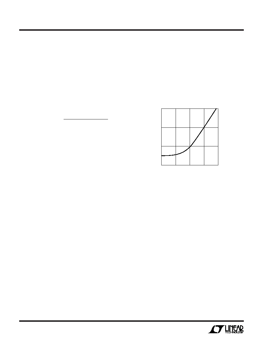
acquisition time (see Figure 6). For minimum acquisition
time with high source impedance, a buffer amplifier should
be used. The only requirement is that the amplifier driving
the analog input(s) must settle after the small current spike
before the next conversion starts (settling time must be
150ns for full throughput rate).
SOURCE RESISTANCE (k
)
0.01
ACQUISITION
TIME
(
s)
1
1415 F06
0.1
0.01
0.1
110
100
10
Figure 6. Acquisition Time vs Source Resistance
Choosing an Input Amplifier
Choosing an input amplifier is easy if a few requirements
are taken into consideration. First, to limit the magnitude
of the voltage spike seen by the amplifier from charging
the sampling capacitor, choose an amplifier that has a
low output impedance (< 100
) at the closed-loop band-
width frequency. For example, if an amplifier is used in a
gain of +1 and has a unity-gain bandwidth of 50MHz, then
the output impedance at 50MHz should be less than
100
. The second requirement is that the closed-loop
bandwidth must be greater than 20MHz to ensure
adequate small-signal settling for full throughput rate. If
slower op amps are used, more settling time can be
provided by increasing the time between conversions.
The best choice for an op amp to drive the LTC1415 will
depend on the application. Generally applications fall into
two categories: AC applications where dynamic specifi-
cations are most critical and time domain applications
where DC accuracy and settling time are most critical.
相关PDF资料 |
PDF描述 |
|---|---|
| AMIS30660CANH2G | TRANSCEIVER CAN HS 5V 8-SOIC |
| VE-J3Y-MY-F2 | CONVERTER MOD DC/DC 3.3V 33W |
| MS3101A18-13P | CONN RCPT 4POS FREE HNG W/PINS |
| AD7862ANZ-10 | IC ADC 12BIT DUAL 250KSPS 28DIP |
| MS3101A16S-4P | CONN RCPT 2POS FREE HNG W/PINS |
相关代理商/技术参数 |
参数描述 |
|---|---|
| LTC1415CSW | 功能描述:IC A/D CONV 12BIT SAMPLNG 28SOIC RoHS:否 类别:集成电路 (IC) >> 数据采集 - 模数转换器 系列:- 标准包装:1,000 系列:- 位数:12 采样率(每秒):300k 数据接口:并联 转换器数目:1 功率耗散(最大):75mW 电压电源:单电源 工作温度:0°C ~ 70°C 安装类型:表面贴装 封装/外壳:24-SOIC(0.295",7.50mm 宽) 供应商设备封装:24-SOIC 包装:带卷 (TR) 输入数目和类型:1 个单端,单极;1 个单端,双极 |
| LTC1415CSW#PBF | 功能描述:IC A/D CONV 12BIT SAMPLNG 28SOIC RoHS:是 类别:集成电路 (IC) >> 数据采集 - 模数转换器 系列:- 标准包装:1 系列:microPOWER™ 位数:8 采样率(每秒):1M 数据接口:串行,SPI? 转换器数目:1 功率耗散(最大):- 电压电源:模拟和数字 工作温度:-40°C ~ 125°C 安装类型:表面贴装 封装/外壳:24-VFQFN 裸露焊盘 供应商设备封装:24-VQFN 裸露焊盘(4x4) 包装:Digi-Reel® 输入数目和类型:8 个单端,单极 产品目录页面:892 (CN2011-ZH PDF) 其它名称:296-25851-6 |
| LTC1415CSW#TR | 功能描述:IC ADC 12BIT 1.25MSPS SMP 28SOIC RoHS:否 类别:集成电路 (IC) >> 数据采集 - 模数转换器 系列:- 标准包装:1,000 系列:- 位数:12 采样率(每秒):300k 数据接口:并联 转换器数目:1 功率耗散(最大):75mW 电压电源:单电源 工作温度:0°C ~ 70°C 安装类型:表面贴装 封装/外壳:24-SOIC(0.295",7.50mm 宽) 供应商设备封装:24-SOIC 包装:带卷 (TR) 输入数目和类型:1 个单端,单极;1 个单端,双极 |
| LTC1415CSW#TRPBF | 功能描述:IC A/D CONV 12BIT SAMPLNG 28SOIC RoHS:是 类别:集成电路 (IC) >> 数据采集 - 模数转换器 系列:- 标准包装:1,000 系列:- 位数:12 采样率(每秒):300k 数据接口:并联 转换器数目:1 功率耗散(最大):75mW 电压电源:单电源 工作温度:0°C ~ 70°C 安装类型:表面贴装 封装/外壳:24-SOIC(0.295",7.50mm 宽) 供应商设备封装:24-SOIC 包装:带卷 (TR) 输入数目和类型:1 个单端,单极;1 个单端,双极 |
| LTC1415CSWPBF | 制造商:Linear Technology 功能描述:LTC1415CSWPBF |
发布紧急采购,3分钟左右您将得到回复。