- 您现在的位置:买卖IC网 > PDF目录2003 > LTC1420IGN#TRPBF (Linear Technology)IC ADC 12BIT 10MSPS SAMPL 28SSOP PDF资料下载
参数资料
| 型号: | LTC1420IGN#TRPBF |
| 厂商: | Linear Technology |
| 文件页数: | 19/20页 |
| 文件大小: | 0K |
| 描述: | IC ADC 12BIT 10MSPS SAMPL 28SSOP |
| 标准包装: | 2,500 |
| 位数: | 12 |
| 采样率(每秒): | 10M |
| 数据接口: | 并联 |
| 转换器数目: | 1 |
| 功率耗散(最大): | 300mW |
| 电压电源: | 单电源 |
| 工作温度: | -40°C ~ 85°C |
| 安装类型: | 表面贴装 |
| 封装/外壳: | 28-SSOP(0.154",3.90mm 宽) |
| 供应商设备封装: | 28-SSOP |
| 包装: | 带卷 (TR) |
| 输入数目和类型: | 2 个单端,双极;1 个差分,双极 |
8
LTC1420
1420fa
Conversion Details
The LTC1420 is a high performance 12-bit A/D converter
that operates up to 10Msps. It is a complete solution with
an on-chip sample-and-hold, a 12-bit pipelined CMOS
ADC, a low drift programmable reference and an input
programmable gain amplifier. The digital output is paral-
lel, with a 12-bit two’s complement output and an out-of-
range (overflow) bit.
The rising edge of the CLK begins a conversion. The
differential analog inputs are simultaneously sampled and
passed on to the pipelined A/D. After two more conversion
starts (plus a 70ns conversion time) the digital outputs are
updated with the conversion result and will be ready for
capture on the third rising clock edge. Thus, even though
a new conversion is begun every time CLK goes high, each
result takes three clock cycles to reach the output.
The analog signals that are passed from stage to stage in
the pipelined A/D are stored on capacitors. The signals on
these capacitors will be lost if the delay between conver-
sions is too long. For accurate conversion results, the part
should be clocked faster than 20kHz.
In some pipelined A/D converters if there is no clock
present, dynamic logic on the chip will droop and the
power consumption sharply increases. The LTC1420
doesn’t have this problem. If the part is not clocked for
500s, an internal timer will refresh the dynamic logic.
Thus, the clock can be turned off for long periods of time
to save power.
Power Supplies
The LTC1420 will operate from either a single 5V or dual
±5V supply, making it easy to interface the analog input to
single or dual supply systems. The digital output drivers
have their own power supply pin (OVDD) which can be set
from 3V to 5V, allowing direct connection to either 3V or
5V digital systems. For single supply operation, VSS should
be connected to analog ground. For dual supply operation,
VSS should be connected to – 5V. Both VDD pins should be
connected to a clean 5V analog supply. (Don’t connect VDD
to a noisy system digital supply.)
Analog Input Ranges
The LTC1420 has a flexible analog input with a wide
selection of input ranges. The input range is always
differential and is set by the voltages at the VREF and the
GAIN pins (Figure 1). The input range of the A/D core is
fixed at ±VREF/2. The reference voltage, VREF, is either set
by the on-chip voltage reference or directly driven by an
external voltage. The GAIN pin is a digital input that
controls the gain of a preamplifier in the sample-and-hold
circuit. The gain of this PGA can be set to 1× or 2×. Table 1
gives the input range in terms of VREF and GAIN.
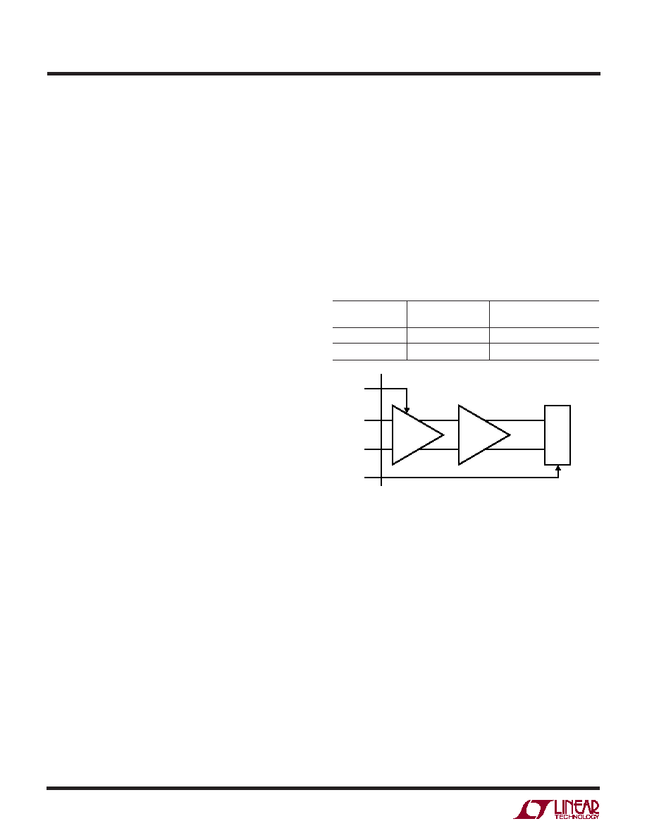
Table 1
INPUT RANGE
GAIN PIN
PGA GAIN
(VIN = AIN+ – AIN–)
5V (Logic H)
1×
–VREF/2 < VIN < VREF/2
OV (Logic L)
2×
–VREF/4 < VIN < VREF/4
VREF
–AIN
+AIN
GAIN
1420 F01
1x/2x
VIN
+
–
±VREF/2
PGA
S/H
ADC
CORE
Internal Reference
Figure 2 shows a simplified schematic of the LTC1420
reference circuitry. An on-chip temperature compensated
bandgap reference (VCM) is factory trimmed to 2.500V.
The voltage at the VREF pin sets the input span of the ADC
to ±VREF/2. An internal voltage divider converts VCM to
2.048V, which is connected to a reference amplifier. The
reference programming pin, SENSE, controls how the
reference amplifier drives the VREF pin. If SENSE is tied to
ground, the reference amplifier feedback is connected to
the R1/R2 voltage divider, thus making VREF = 4.096V. If
SENSE is tied to VREF, the reference amplifier feedback is
connected to SENSE thus making VREF = 2.048V. If SENSE
is tied to VDD, the reference amplifier is disconnected from
Figure 1. Analog Input Circuit
APPLICATIONS INFORMATION
WU
U
相关PDF资料 |
PDF描述 |
|---|---|
| LTC1426IS8#TR | IC DAC PWM 6BIT DUAL MCPWR 8SOIC |
| LTC1427CS8-50#TRPBF | IC D/A CONV 10BIT W/SMBUS 8-SOIC |
| LTC1428CS8-50#TRPBF | IC D/A CONV 8BIT SINK OUT 8-SOIC |
| LTC1446LIS8#TRPBF | IC D/A CONV 12BIT R-R DUAL 8SOIC |
| LTC1448IS8#TRPBF | IC D/A CONV 12BIT R-R DUAL 8SOIC |
相关代理商/技术参数 |
参数描述 |
|---|---|
| LTC1421CG | 功能描述:IC CONTROLLER HOT SWAP 24-SSOP RoHS:否 类别:集成电路 (IC) >> PMIC - 热交换 系列:- 产品培训模块:Lead (SnPb) Finish for COTS Obsolescence Mitigation Program 标准包装:119 系列:- 类型:热交换控制器 应用:通用型,PCI Express? 内部开关:无 电流限制:- 电源电压:3.3V,12V 工作温度:-40°C ~ 85°C 安装类型:表面贴装 封装/外壳:80-TQFP 供应商设备封装:80-TQFP(12x12) 包装:托盘 产品目录页面:1423 (CN2011-ZH PDF) |
| LTC1421CG#PBF | 功能描述:IC CONTROLLER HOT SWAP 24-SSOP RoHS:是 类别:集成电路 (IC) >> PMIC - 热交换 系列:- 产品培训模块:Lead (SnPb) Finish for COTS Obsolescence Mitigation Program 标准包装:119 系列:- 类型:热交换控制器 应用:通用型,PCI Express? 内部开关:无 电流限制:- 电源电压:3.3V,12V 工作温度:-40°C ~ 85°C 安装类型:表面贴装 封装/外壳:80-TQFP 供应商设备封装:80-TQFP(12x12) 包装:托盘 产品目录页面:1423 (CN2011-ZH PDF) |
| LTC1421CG#TR | 功能描述:IC CONTROLLER HOTSWAP ADJ 24SSOP RoHS:否 类别:集成电路 (IC) >> PMIC - 热交换 系列:- 产品培训模块:Lead (SnPb) Finish for COTS Obsolescence Mitigation Program 标准包装:119 系列:- 类型:热交换控制器 应用:通用型,PCI Express? 内部开关:无 电流限制:- 电源电压:3.3V,12V 工作温度:-40°C ~ 85°C 安装类型:表面贴装 封装/外壳:80-TQFP 供应商设备封装:80-TQFP(12x12) 包装:托盘 产品目录页面:1423 (CN2011-ZH PDF) |
| LTC1421CG#TRPBF | 功能描述:IC CONTROLLER HOT SWAP 24-SSOP RoHS:是 类别:集成电路 (IC) >> PMIC - 热交换 系列:- 产品培训模块:Lead (SnPb) Finish for COTS Obsolescence Mitigation Program 标准包装:119 系列:- 类型:热交换控制器 应用:通用型,PCI Express? 内部开关:无 电流限制:- 电源电压:3.3V,12V 工作温度:-40°C ~ 85°C 安装类型:表面贴装 封装/外壳:80-TQFP 供应商设备封装:80-TQFP(12x12) 包装:托盘 产品目录页面:1423 (CN2011-ZH PDF) |
| LTC1421CG1 | 制造商:Linear Technology 功能描述: |
发布紧急采购,3分钟左右您将得到回复。