- 您现在的位置:买卖IC网 > PDF目录19870 > LTC1422CS8#TRPBF (Linear Technology)IC CONTROLLER HOT SWAP 8-SOIC PDF资料下载
参数资料
| 型号: | LTC1422CS8#TRPBF |
| 厂商: | Linear Technology |
| 文件页数: | 7/16页 |
| 文件大小: | 197K |
| 描述: | IC CONTROLLER HOT SWAP 8-SOIC |
| 标准包装: | 2,500 |
| 类型: | 热交换控制器 |
| 应用: | 通用 |
| 内部开关: | 无 |
| 电源电压: | 2.7 V ~ 12 V |
| 工作温度: | 0°C ~ 70°C |
| 安装类型: | 表面贴装 |
| 封装/外壳: | 8-SOIC(0.154",3.90mm 宽) |
| 供应商设备封装: | 8-SOIC |
| 包装: | 带卷 (TR) |
7
LTC1422
1422fb
APPLICATIONS INFORMATION
U
U
U
Hot Circuit Insertion
When circuit boards are inserted into a live backplane, the
supply bypass capacitors on the board can draw huge
transient currents from the backplane power bus as they
charge up. The transient currents can cause permanent
damage to the connector pins and cause glitches on the
system supply, causing other boards in the system to
reset.
The LTC1422 is designed to turn a boards supply voltage
on and off in a controlled manner, allowing the board to be
safely inserted or removed from a live backplane. The chip
also provides a system reset signal to indicate when board
supply voltage drops below a programmable voltage.
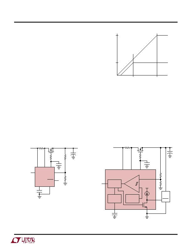
Power Supply Ramping
The onboard power supply is controlled by placing an
external N-channel pass transistor in the power path
(Figure 1). R1 provides current fault detection and R2
prevents high frequency oscillation. By ramping up the
gate of the pass transistor at a controlled rate, the transient
surge current (I = C " dV/dt) drawn from the main backplane
supply can be limited to a safe value when the board makes
connection.
V
CC
+ 10V
V
CC
1422 F02
t
1
t
2
GATE
V
OUT
SLOPE = 10礎/C1
Figure 2. Supply Turn-On
Figure 3. Supply Monitor Block Diagram
equal to 10礎/C1
(Figure 2), where C1
is the external
capacitor connected between the GATE pin and GND.
The ramp time for the supply is equal to: t = (V
CC
" C1)/
10礎. After the ON pin has been pulled low for more than
40祍, the GATE is immediately pulled to GND.
Voltage Monitor
The LTC1422 uses a 1.232V bandgap reference, precision
voltage comparator and a resistive divider to monitor the
output supply voltage (Figure 3).
Figure 1. Supply Control Circuitry
+
V
CC
SENSE
TIMER
GND
GATE
LTC1422
ON
8
3
4
7
6
C1
C
LOAD
C2
R3
V
OUT
V
CC
Q1
R1
5
2
1422F01
1
FB
RESET
R2
10&
R4
When power is first applied to the chip, the gate of the
N-channel (Pin 6) is pulled low. After the ON pin is held
high for at least one timing cycle, the charge pump is
turned on. The voltage at GATE begins to rise with a slope
+
SENSE
12礎
R4
R3
7
V
CC
V
OUT
V
CC
8
GATE
LTC1422
6
2
FB
Q2
ON
1422 F03
1
5
C2
3
4
C1
C
LOAD
Q1
R1
LOGIC
TIMER
1.232V
REFERENCE
+
COMP 2
礟
RESET
R2
相关PDF资料 |
PDF描述 |
|---|---|
| VI-B1J-CY-F2 | CONVERTER MOD DC/DC 36V 50W |
| ATF1504ASVL-20JU44 | IC CPLD 20NS LOWV LOW PWR 44PLCC |
| VI-B1J-CY-F1 | CONVERTER MOD DC/DC 36V 50W |
| ATF1508ASV-15JU84 | IC CPLD 15NS LOW V 84PLCC |
| VI-21J-CY-F3 | CONVERTER MOD DC/DC 36V 50W |
相关代理商/技术参数 |
参数描述 |
|---|---|
| LTC1422IN8 | 功能描述:IC CONTROLLER HOT SWAP 8-DIP RoHS:否 类别:集成电路 (IC) >> PMIC - 热交换 系列:- 产品培训模块:Obsolescence Mitigation Program 标准包装:100 系列:- 类型:热插拔开关 应用:通用 内部开关:是 电流限制:可调 电源电压:9 V ~ 13.2 V 工作温度:-40°C ~ 150°C 安装类型:表面贴装 封装/外壳:10-WFDFN 裸露焊盘 供应商设备封装:10-TDFN-EP(3x3) 包装:管件 |
| LTC1422IN8#PBF | 功能描述:IC CONTROLLER HOT SWAP 8-DIP RoHS:是 类别:集成电路 (IC) >> PMIC - 热交换 系列:- 产品培训模块:Obsolescence Mitigation Program 标准包装:100 系列:- 类型:热插拔开关 应用:通用 内部开关:是 电流限制:可调 电源电压:9 V ~ 13.2 V 工作温度:-40°C ~ 150°C 安装类型:表面贴装 封装/外壳:10-WFDFN 裸露焊盘 供应商设备封装:10-TDFN-EP(3x3) 包装:管件 |
| LTC1422IS8 | 功能描述:IC CONTROLLER HOT SWAP 8-SOIC RoHS:否 类别:集成电路 (IC) >> PMIC - 热交换 系列:- 产品培训模块:Obsolescence Mitigation Program 标准包装:100 系列:- 类型:热插拔开关 应用:通用 内部开关:是 电流限制:可调 电源电压:9 V ~ 13.2 V 工作温度:-40°C ~ 150°C 安装类型:表面贴装 封装/外壳:10-WFDFN 裸露焊盘 供应商设备封装:10-TDFN-EP(3x3) 包装:管件 |
| LTC1422IS8#PBF | 功能描述:IC CONTROLLER HOT SWAP 8-SOIC RoHS:是 类别:集成电路 (IC) >> PMIC - 热交换 系列:- 标准包装:50 系列:- 类型:热交换控制器 应用:-48V 远程电力系统,AdvancedTCA ? 系统,高可用性 内部开关:无 电流限制:可调 电源电压:11.5 V ~ 14.5 V 工作温度:-40°C ~ 85°C 安装类型:表面贴装 封装/外壳:10-TFSOP,10-MSOP(0.118",3.00mm 宽) 供应商设备封装:10-MSOP 包装:管件 |
| LTC1422IS8#TR | 功能描述:IC CONTROLLER HOTSWAP 8SOIC RoHS:否 类别:集成电路 (IC) >> PMIC - 热交换 系列:- 产品培训模块:Obsolescence Mitigation Program 标准包装:100 系列:- 类型:热插拔开关 应用:通用 内部开关:是 电流限制:可调 电源电压:9 V ~ 13.2 V 工作温度:-40°C ~ 150°C 安装类型:表面贴装 封装/外壳:10-WFDFN 裸露焊盘 供应商设备封装:10-TDFN-EP(3x3) 包装:管件 |
发布紧急采购,3分钟左右您将得到回复。