- 您现在的位置:买卖IC网 > PDF目录15258 > LTC1436ACGN-PLL#TRPBF (Linear Technology)IC REG CTRLR BUCK PWM CM 24-SSOP PDF资料下载
参数资料
| 型号: | LTC1436ACGN-PLL#TRPBF |
| 厂商: | Linear Technology |
| 文件页数: | 21/28页 |
| 文件大小: | 0K |
| 描述: | IC REG CTRLR BUCK PWM CM 24-SSOP |
| 标准包装: | 2,500 |
| PWM 型: | 电流模式 |
| 输出数: | 1 |
| 频率 - 最大: | 138kHz |
| 占空比: | 99% |
| 电源电压: | 3.5 V ~ 30 V |
| 降压: | 是 |
| 升压: | 无 |
| 回扫: | 无 |
| 反相: | 无 |
| 倍增器: | 无 |
| 除法器: | 无 |
| Cuk: | 无 |
| 隔离: | 无 |
| 工作温度: | 0°C ~ 70°C |
| 封装/外壳: | 24-SSOP(0.154",3.90mm 宽) |
| 包装: | 带卷 (TR) |
第1页第2页第3页第4页第5页第6页第7页第8页第9页第10页第11页第12页第13页第14页第15页第16页第17页第18页第19页第20页当前第21页第22页第23页第24页第25页第26页第27页第28页
�� �
�
�LTC1436A�
�LTC1436A-PLL/LTC1437A�
�APPLICATIO� N� S� I� N� FOR� M� ATIO� N�
�Efficiency.� For� example,� in� a� 20V� to� 5V� application,�
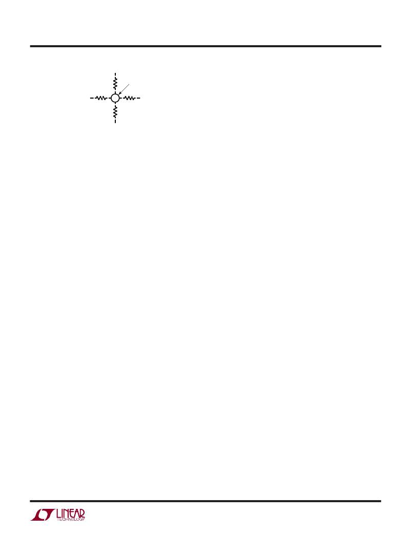
�INDUCTOR�
�L�
�1435A� F08�
�Figure� 13.� Allowable� Inductor/R� SENSE� Layout� Orientations�
�Efficiency� Considerations�
�The� efficiency� of� a� switching� regulator� is� equal� to� the�
�output� power� divided� by� the� input� power� times� 100%.� It� is�
�often� useful� to� analyze� individual� losses� to� determine� what�
�is� limiting� the� efficiency� and� which� change� would� produce�
�the� most� improvement.� Efficiency� can� be� expressed� as:�
�Efficiency� =� 100%� –� (L1� +� L2� +� L3� +� ...)�
�where� L1,� L2,� etc.� are� the� individual� losses� as� a� percentage�
�of� input� power.�
�Although� all� dissipative� elements� in� the� circuit� produce�
�losses,� four� main� sources� usually� account� for� most� of� the�
�losses� in� LTC1436A/LTC1437A� circuits:� LTC1436A/�
�LTC1437A� V� IN� current,� INTV� CC� current,� I� 2� R� losses� and�
�topside� MOSFET� transition� losses.�
�1.� The� V� IN� current� is� the� DC� supply� current� given� in� the�
�Electrical� Characteristics� table� which� excludes� MOSFET�
�driver� and� control� currents.� V� IN� current� results� in� a�
�small� (<� 1%)� loss� which� increases� with� V� IN� .�
�2.� INTV� CC� current� is� the� sum� of� the� MOSFET� driver� and�
�control� currents.� The� MOSFET� driver� current� results�
�from� switching� the� gate� capacitance� of� the� power�
�MOSFETs.� Each� time� a� MOSFET� gate� is� switched� from�
�low� to� high� to� low� again,� a� packet� of� charge� dQ� moves�
�from� INTV� CC� to� ground.� The� resulting� dQ/dt� is� a� current�
�out� of� INTV� CC� that� is� typically� much� larger� than� the�
�control� circuit� current.� In� continuous� mode,� I� GATECHG� =�
�f(Q� T� +� Q� B� ),� where� Q� T� and� Q� B� are� the� gate� charges� of� the�
�topside� and� bottom� side� MOSFETs.� It� is� for� this� reason�
�that� the� Adaptive� Power� output� stage� switches� to� a� low�
�Q� T� MOSFET� during� low� current� operation.�
�By� powering� EXTV� CC� from� an� output-derived� source,�
�the� additional� V� IN� current� resulting� from� the� driver� and�
�control� currents� will� be� scaled� by� a� factor� of� Duty� Cycle/�
�10mA� of� INTV� CC� current� results� in� approximately� 3mA�
�of� V� IN� current.� This� reduces� the� midcurrent� loss� from�
�10%� or� more� (if� the� driver� was� powered� directly� from�
�V� IN� )� to� only� a� few� percent.�
�3.� I� 2� R� losses� are� predicted� from� the� DC� resistances� of� the�
�MOSFET,� inductor� and� current� shunt.� In� continuous�
�mode� the� average� output� current� flows� through� L� and�
�R� SENSE� ,� but� is� “chopped”� between� the� topside� main�
�MOSFET� and� the� synchronous� MOSFET.� If� the� two�
�MOSFETs� have� approximately� the� same� R� DS(ON)� ,� then�
�the� resistance� of� one� MOSFET� can� simply� be� summed�
�with� the� resistances� of� L� and� R� SENSE� to� obtain� I� 2� R�
�losses.� For� example,� if� each� R� DS(ON)� =� 0.05� ?� ,�
�R� L� =� 0.15� ?� and� R� SENSE� =� 0.05� ?� ,� then� the� total� resis-�
�tance� is� 0.25� ?� .� This� results� in� losses� ranging� from� 3%�
�to� 10%� as� the� output� current� increases� from� 0.5A� to� 2A.�
�I� 2� R� losses� cause� the� efficiency� to� drop� at� high� output�
�currents.�
�4.� Transition� losses� apply� only� to� the� topside� MOSFET(s),�
�and� only� when� operating� at� high� input� voltages� (typi-�
�cally� 20V� or� greater).� Transition� losses� can� be� esti-�
�mated� from:�
�Transition� Loss� =� 2.5(V� IN� )� 1.85� (I� MAX� )(C� RSS� )(f)�
�Other� losses� including� C� IN� and� C� OUT� ESR� dissipative�
�losses,� Schottky� conduction� losses� during� dead-time� and�
�inductor� core� losses,� generally� account� for� less� than� 2%�
�total� additional� loss.�
�Checking� Transient� Response�
�The� regulator� loop� response� can� be� checked� by� looking� at�
�the� load� transient� response.� Switching� regulators� take�
�several� cycles� to� respond� to� a� step� in� DC� (resistive)� load�
�current.� When� a� load� step� occurs,� V� OUT� immediately� shifts�
�by� an� amount� equal� to� (� ?� I� LOAD� )(ESR),� where� ESR� is� the�
�effective� series� resistance� of� C� OUT� .� ?� I� LOAD� also� begins� to�
�charge� or� discharge� C� OUT� which� generates� a� feedback�
�error� signal.� The� regulator� loop� then� acts� to� return� V� OUT� to�
�its� steady-state� value.� During� this� recovery� time� V� OUT� can�
�be� monitored� for� overshoot� or� ringing,� which� would�
�indicate� a� stability� problem.� The� I� TH� external� components�
�shown� in� the� Figure� 1� circuit� will� provide� adequate� com-�
�pensation� for� most� applications.�
�14367afb�
�21�
�相关PDF资料 |
PDF描述 |
|---|---|
| VE-B5V-EV-F4 | CONVERTER MOD DC/DC 5.8V 150W |
| LTC1628IG#TRPBF | IC REG CTRLR BUCK PWM CM 28-SSOP |
| VE-B5V-EV-F2 | CONVERTER MOD DC/DC 5.8V 150W |
| URZ1C332MHD | CAP ALUM 3300UF 16V 20% RADIAL |
| VE-B5W-EV-F4 | CONVERTER MOD DC/DC 5.5V 150W |
相关代理商/技术参数 |
参数描述 |
|---|---|
| LTC1436AEGN#PBF | 功能描述:IC REG CTRLR BUCK PWM CM 24-SSOP RoHS:是 类别:集成电路 (IC) >> PMIC - 稳压器 - DC DC 切换控制器 系列:- 标准包装:4,000 系列:- PWM 型:电压模式 输出数:1 频率 - 最大:1.5MHz 占空比:66.7% 电源电压:4.75 V ~ 5.25 V 降压:是 升压:无 回扫:无 反相:无 倍增器:无 除法器:无 Cuk:无 隔离:无 工作温度:-40°C ~ 85°C 封装/外壳:40-VFQFN 裸露焊盘 包装:带卷 (TR) |
| LTC1436AEGN#TRPBF | 功能描述:IC REG CTRLR BUCK PWM CM 24-SSOP RoHS:是 类别:集成电路 (IC) >> PMIC - 稳压器 - DC DC 切换控制器 系列:- 标准包装:4,000 系列:- PWM 型:电压模式 输出数:1 频率 - 最大:1.5MHz 占空比:66.7% 电源电压:4.75 V ~ 5.25 V 降压:是 升压:无 回扫:无 反相:无 倍增器:无 除法器:无 Cuk:无 隔离:无 工作温度:-40°C ~ 85°C 封装/外壳:40-VFQFN 裸露焊盘 包装:带卷 (TR) |
| LTC1436AIGN | 功能描述:IC REG CTRLR BUCK PWM CM 24-SSOP RoHS:否 类别:集成电路 (IC) >> PMIC - 稳压器 - DC DC 切换控制器 系列:- 标准包装:4,500 系列:PowerWise® PWM 型:控制器 输出数:1 频率 - 最大:1MHz 占空比:95% 电源电压:2.8 V ~ 5.5 V 降压:是 升压:无 回扫:无 反相:无 倍增器:无 除法器:无 Cuk:无 隔离:无 工作温度:-40°C ~ 125°C 封装/外壳:6-WDFN 裸露焊盘 包装:带卷 (TR) 配用:LM1771EVAL-ND - BOARD EVALUATION LM1771 其它名称:LM1771SSDX |
| LTC1436AIGN#PBF | 功能描述:IC REG CTRLR BUCK PWM CM 24-SSOP RoHS:是 类别:集成电路 (IC) >> PMIC - 稳压器 - DC DC 切换控制器 系列:- 标准包装:4,500 系列:PowerWise® PWM 型:控制器 输出数:1 频率 - 最大:1MHz 占空比:95% 电源电压:2.8 V ~ 5.5 V 降压:是 升压:无 回扫:无 反相:无 倍增器:无 除法器:无 Cuk:无 隔离:无 工作温度:-40°C ~ 125°C 封装/外壳:6-WDFN 裸露焊盘 包装:带卷 (TR) 配用:LM1771EVAL-ND - BOARD EVALUATION LM1771 其它名称:LM1771SSDX |
| LTC1436AIGN#TR | 功能描述:IC REG CTRLR BUCK PWM CM 24-SSOP RoHS:否 类别:集成电路 (IC) >> PMIC - 稳压器 - DC DC 切换控制器 系列:- 标准包装:4,500 系列:PowerWise® PWM 型:控制器 输出数:1 频率 - 最大:1MHz 占空比:95% 电源电压:2.8 V ~ 5.5 V 降压:是 升压:无 回扫:无 反相:无 倍增器:无 除法器:无 Cuk:无 隔离:无 工作温度:-40°C ~ 125°C 封装/外壳:6-WDFN 裸露焊盘 包装:带卷 (TR) 配用:LM1771EVAL-ND - BOARD EVALUATION LM1771 其它名称:LM1771SSDX |
发布紧急采购,3分钟左右您将得到回复。