- 您现在的位置:买卖IC网 > PDF目录14118 > LTC1502IS8-3.3#TR (Linear Technology)IC REG SWITCHED CAP 3.3V 8SOIC PDF资料下载
参数资料
| 型号: | LTC1502IS8-3.3#TR |
| 厂商: | Linear Technology |
| 文件页数: | 5/8页 |
| 文件大小: | 0K |
| 描述: | IC REG SWITCHED CAP 3.3V 8SOIC |
| 标准包装: | 2,500 |
| 类型: | 切换式电容器(充电泵) |
| 输出类型: | 固定 |
| 输出数: | 1 |
| 输出电压: | 3.3V |
| 输入电压: | 0.9 V ~ 1.8 V |
| 频率 - 开关: | 500kHz |
| 电流 - 输出: | 10mA |
| 同步整流器: | 无 |
| 工作温度: | -40°C ~ 85°C |
| 安装类型: | 表面贴装 |
| 封装/外壳: | 8-SOIC(0.154",3.90mm 宽) |
| 包装: | 带卷 (TR) |
| 供应商设备封装: | 8-SOIC |
�� �
�
�LTC1502-3.3�
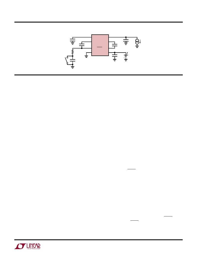
�TEST� CIRCUIT�
�10� μ� F�
�1� μ� F�
�1�
�2�
�3�
�C2� V� OUT�
�C1� +� C3� +�
�LTC1502-3.3�
�C1� –� /SHDN� C3� –�
�8�
�7�
�6�
�1� μ� F�
�10� μ� F�
�I� OUT�
�SWITCH�
�100� ?�
�4�
�GND�
�V� IN�
�5�
�10� μ� F�
�V� IN�
�CLOSED� FOR�
�100pF�
�SHUTDOWN�
�1502-3.3� TC�
�APPLICATIO� N� S� I� N� FOR� M� ATIO� N�
�Regulator� Operation�
�The� LTC1502-3.3� uses� a� quadrupler� charge� pump� DC/DC�
�converter� to� produce� a� boosted� output� voltage.� The�
�quadrupler� charge� pump� consists� of� two� voltage� doubler�
�charge� pumps� (CP1� and� CP2� on� the� Block� Diagram)�
�cascaded� in� series.� CP1� doubles� the� input� voltage� V� IN� and�
�the� CP1� output� voltage� is� stored� on� external� capacitor� C2.�
�The� C2� pin� also� serves� as� the� input� for� doubler� CP2� whose�
�output� is� stored� on� the� output� capacitor� C� OUT� .� Each�
�doubler� is� controlled� by� a� two-phase� clock� which� is�
�generated� in� the� Timing� Control� circuit.� On� phase� one� of�
�the� clock,� the� flying� capacitors� C1� and� C3� are� charged� to�
�their� respective� input� voltages.� On� phase� two� each� charged�
�flying� capacitor� is� stacked� on� top� of� the� input� voltage� and�
�discharged� through� an� internal� switch� onto� its� respective�
�output.� This� sequence� of� charging� and� discharging� the�
�CP1� and� CP2� flying� capacitors� continues� at� the� free�
�running� oscillator� frequency� (500kHz� typ)� until� the� output�
�is� in� regulation.�
�Regulation� is� achieved� by� comparing� the� divided� down�
�output� voltage� to� a� fixed� voltage� reference.� The� charge�
�pump� clocks� are� disabled� when� the� output� voltage� is�
�above� the� desired� regulation� point� set� by� COMP1.� When�
�the� output� has� dropped� below� the� lower� trip� point� of�
�COMP1,� the� charge� pump� clocks� are� turned� back� on� until�
�V� OUT� is� boosted� back� into� regulation.�
�Enhanced� Start-Up�
�Enhanced� start-up� capability� is� provided� by� the� COMP2�
�circuitry.� COMP2� compares� the� divided� down� C2� voltage�
�to� the� input� voltage� V� IN� .� The� COMP2� output� disables� the�
�output� charge� pump� CP2� whenever� the� divided� C2� voltage�
�is� lower� than� V� IN� .� The� CP2� output� is� thereby� forced� into� a�
�high� impedance� state� until� the� voltage� on� C2� has� been�
�raised� above� V� IN� (the� C2� pin� should� not� be� loaded� for�
�proper� start-up).� This� allows� a� higher� internal� gate� drive�
�voltage� to� be� generated� (from� the� C2� pin)� before� the� output�
�(V� OUT� )� is� connected� to� a� load.� Hysteresis� in� COMP2� forces�
�CP2� to� be� turned� ON� and� OFF� while� C� OUT� is� charging� up� to�
�prevent� a� lockup� condition� if� C2� droops� too� low� during�
�start-up.� By� the� time� the� output� nears� the� regulation� point,�
�the� C2� voltage� is� well� above� the� lower� trip� point� of� COMP2�
�and� CP2� will� remain� enabled.� This� method� of� disabling� the�
�output� charge� pump� while� an� internal� boosted� gate� drive�
�supply� is� developed� allows� the� part� to� start� up� at� low�
�voltages� with� a� larger� output� current� load� than� would�
�otherwise� be� possible.�
�Shutdown�
�Shutdown� is� implemented� using� an� external� pull-down�
�device� on� the� C1� –� /SHDN� pin.� The� recommended� external�
�pull-down� device� is� an� open-drain� FET� with� resistive� cur-�
�rent� limiting� (see� Figure� 1).� The� pull-down� device� must� sink�
�up� to� 300� μ� A� and� pull� down� below� 0.2V� to� ensure� proper�
�shutdown� operation,� however,� the� actual� series� resistance�
�is� not� critical.� The� pull-down� device� must� also� go� into� a� Hi-�
�Z� state� for� the� LTC1502-3.3� to� become� active.�
�The� timing� control� circuitry� forces� the� CP1� switches� into�
�a� high� impedance� state� every� 16� clock� cycles.� The� Hi-Z�
�duration� is� equal� to� one� clock� cycle.� At� the� end� of� the�
�Hi-Z� time� interval,� the� voltage� on� the� C1� –� /SHDN� pin� is�
�sampled.� If� the� C1� –� /SHDN� pin� has� been� pulled� to� a� logic�
�low� state,� the� part� will� go� into� shutdown� mode.� When� the�
�pull-down� device� is� disabled,� an� internal� pull-up� current�
�5�
�相关PDF资料 |
PDF描述 |
|---|---|
| SDR0602-150ML | INDUCTOR 15UH 800MA SMD |
| HCC20DRTS | CONN EDGECARD 40POS DIP .100 SLD |
| VE-J0P-CZ-F2 | CONVERTER MOD DC/DC 13.8V 25W |
| GMC18DRXS | CONN EDGECARD 36POS DIP .100 SLD |
| VE-J0P-CZ-F1 | CONVERTER MOD DC/DC 13.8V 25W |
相关代理商/技术参数 |
参数描述 |
|---|---|
| LTC1503CMS8-1.8 | 功能描述:IC REG BUCK SWITCHED CAP 8MSOP RoHS:否 类别:集成电路 (IC) >> PMIC - 稳压器 - DC DC 开关稳压器 系列:- 标准包装:2,500 系列:- 类型:升压(升压) 输出类型:可调式 输出数:1 输出电压:1.24 V ~ 30 V 输入电压:1.5 V ~ 12 V PWM 型:电流模式,混合 频率 - 开关:600kHz 电流 - 输出:500mA 同步整流器:无 工作温度:-40°C ~ 85°C 安装类型:表面贴装 封装/外壳:8-SOIC(0.154",3.90mm 宽) 包装:带卷 (TR) 供应商设备封装:8-SOIC |
| LTC1503CMS8-1.8#PBF | 功能描述:IC REG BUCK SWITCHED CAP 8MSOP RoHS:是 类别:集成电路 (IC) >> PMIC - 稳压器 - DC DC 开关稳压器 系列:- 标准包装:2,500 系列:- 类型:升压(升压) 输出类型:可调式 输出数:1 输出电压:1.24 V ~ 30 V 输入电压:1.5 V ~ 12 V PWM 型:电流模式,混合 频率 - 开关:600kHz 电流 - 输出:500mA 同步整流器:无 工作温度:-40°C ~ 85°C 安装类型:表面贴装 封装/外壳:8-SOIC(0.154",3.90mm 宽) 包装:带卷 (TR) 供应商设备封装:8-SOIC |
| LTC1503CMS8-1.8#PBF | 制造商:Linear Technology 功能描述:DC/DC Charge Pump Converter IC |
| LTC1503CMS8-1.8#TR | 功能描述:IC REG BUCK SWITCHED CAP 8MSOP RoHS:否 类别:集成电路 (IC) >> PMIC - 稳压器 - DC DC 开关稳压器 系列:- 标准包装:2,500 系列:- 类型:升压(升压) 输出类型:可调式 输出数:1 输出电压:1.24 V ~ 30 V 输入电压:1.5 V ~ 12 V PWM 型:电流模式,混合 频率 - 开关:600kHz 电流 - 输出:500mA 同步整流器:无 工作温度:-40°C ~ 85°C 安装类型:表面贴装 封装/外壳:8-SOIC(0.154",3.90mm 宽) 包装:带卷 (TR) 供应商设备封装:8-SOIC |
| LTC1503CMS8-1.8#TRPBF | 功能描述:IC REG BUCK SWITCHED CAP 8MSOP RoHS:是 类别:集成电路 (IC) >> PMIC - 稳压器 - DC DC 开关稳压器 系列:- 标准包装:2,500 系列:- 类型:升压(升压) 输出类型:可调式 输出数:1 输出电压:1.24 V ~ 30 V 输入电压:1.5 V ~ 12 V PWM 型:电流模式,混合 频率 - 开关:600kHz 电流 - 输出:500mA 同步整流器:无 工作温度:-40°C ~ 85°C 安装类型:表面贴装 封装/外壳:8-SOIC(0.154",3.90mm 宽) 包装:带卷 (TR) 供应商设备封装:8-SOIC |
发布紧急采购,3分钟左右您将得到回复。