- 您现在的位置:买卖IC网 > PDF目录44988 > LTC1530IS8-2.5#PBF (LINEAR TECHNOLOGY CORP) SWITCHING CONTROLLER, 350 kHz SWITCHING FREQ-MAX, PDSO8 PDF资料下载
参数资料
| 型号: | LTC1530IS8-2.5#PBF |
| 厂商: | LINEAR TECHNOLOGY CORP |
| 元件分类: | 稳压器 |
| 英文描述: | SWITCHING CONTROLLER, 350 kHz SWITCHING FREQ-MAX, PDSO8 |
| 封装: | 0.150 INCH, PLASTIC, SO-8 |
| 文件页数: | 3/24页 |
| 文件大小: | 301K |
| 代理商: | LTC1530IS8-2.5#PBF |
11
LTC1530
1530fa
Power MOSFETs
Two N-channel power MOSFETs are required for synchro-
nous LTC1530 circuits. They should be selected based
primarily on threshold voltage and on-resistance consid-
erations. Thermal dissipation is often a secondary con-
cern in high efficiency designs. The required MOSFET
threshold should be determined based on the available
power supply voltages and/or the complexity of the gate
drive charge pump scheme. In 5V input designs where a
12V supply is used to power PVCC, standard MOSFETs
with RDS(ON) specified at VGS = 5V or 6V can be used with
good results. The current drawn from the 12V supply
varies with the MOSFETs used and the LTC1530’s operat-
ing frequency, but is generally less than 50mA.
LTC1530 applications that use a 5V VIN voltage and a
doubling charge pump to generate PVCC do not provide
enough gate drive voltage to fully enhance standard
power MOSFETs. Under this condition, the effective
MOSFET RDS(ON) may be quite high, raising the dissipa-
tion in the FETs and reducing efficiency. In addition,
power supply start-up problems can occur with standard
power MOSFETs. These start-up problems can occur for
two reasons. First, if the MOSFET is not fully enhanced,
the higher effective RDS(ON) causes the LTC1530 to acti-
vate current limit at a much lower level than the desired
trip point. Second, standard MOSFETs have higher GATE
threshold voltages than logic level MOSFETs, thereby
increasing the PVCC voltage required to turn them on. A
MOSFET whose RDS(ON) is rated at VGS = 4.5V does not
necessarily have a logic level MOSFET GATE threshold
voltage. Logic level FETs are the recommended choice for
5V-only systems. Logic level FETs can be fully enhanced
with a doubler charge pump and will operate at maximum
efficiency. Note that doubler charge pump designs run-
ning from supplies higher than 6.5V should include a
Zener diode clamp at PVCC to prevent transients from
exceeding the absolute maximum rating of the pin.
After the MOSFET threshold voltage is selected, choose
the RDS(ON) based on the input voltage, the output voltage,
allowable power dissipation and maximum output cur-
rent. In a typical LTC1530 buck converter circuit, operat-
ing in continuous mode, the average inductor current is
equal to the output load current. This current flows through
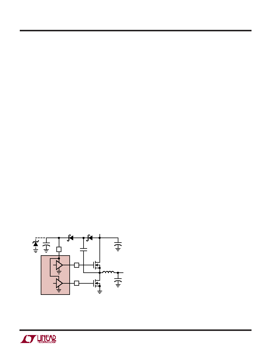
+
0.22
F
10
F
+
CO
CIN
LO
MBR0530T1 MBR0530T1
OPTIONAL FOR
VIN > 6.5V
LTC1530
PVCC
G1
VOUT
1530 F07
VIN
13V
1N5243B
Q1
Q2
G2
In order for the current limit circuit to operate properly and
to obtain a reasonably accurate current limit threshold, the
IMAX and IFB pins must be Kelvin sensed at Q1’s drain and
source pins. A 0.1
F decoupling capacitor can also be
connected across RIMAX to filter switching noise. In addi-
tion, LTC recommends that the voltage drop across the
RIMAX resistor be set to ≥100mV. Otherwise, noise spikes
or ringing at Q1’s source can cause the actual current limit
to be greater than the desired current limit set point.
MOSFET Gate Drive
The PVCC supply must be greater than the input supply
voltage, VIN, by at least one power MOSFET VGS(ON) for
efficient operation. This higher voltage can be supplied
with a separate supply, or it can be generated using a
simple charge pump as shown in Figure 7. The 86%
maximum duty cycle ensures sufficient off-time to refresh
the charge pump during each cycle.
As PVCC is powered up from 0V, the LTC1530 undervolt-
age lockout circuit prevents G1 and G2 from pulling high
until PVCC reaches about 3.5V. To prevent Q1’s high
RDS(ON) from triggering the current limit comparator while
PVCC is slewing, the current limit circuit is disabled until
PVCC is≥8V. In addition, on start-up or recovery from
thermal shutdown, the driver logic is designed to hold G2
low until G1 first goes high.
Figure 7. Doubling Charge Pump
APPLICATIO S I FOR ATIO
WU
UU
相关PDF资料 |
PDF描述 |
|---|---|
| LTC1530CS8-2.8#TR | SWITCHING CONTROLLER, 350 kHz SWITCHING FREQ-MAX, PDSO8 |
| LTC1628IG#PBF | 3 A SWITCHING CONTROLLER, 310 kHz SWITCHING FREQ-MAX, PDSO28 |
| LTC1628IG-SYNC#TR | 3 A SWITCHING CONTROLLER, 360 kHz SWITCHING FREQ-MAX, PDSO28 |
| LTC1643HCGN#PBF | 4-CHANNEL POWER SUPPLY SUPPORT CKT, PDSO16 |
| LTC1643LCGN#TR | 4-CHANNEL POWER SUPPLY SUPPORT CKT, PDSO16 |
相关代理商/技术参数 |
参数描述 |
|---|---|
| LTC1530IS8-3.3 | 功能描述:IC SW REG CNTRLR SYNC 3.3V 8SOIC RoHS:否 类别:集成电路 (IC) >> PMIC - 稳压器 - 专用型 系列:- 标准包装:43 系列:- 应用:控制器,Intel VR11 输入电压:5 V ~ 12 V 输出数:1 输出电压:0.5 V ~ 1.6 V 工作温度:-40°C ~ 85°C 安装类型:表面贴装 封装/外壳:48-VFQFN 裸露焊盘 供应商设备封装:48-QFN(7x7) 包装:管件 |
| LTC1530IS8-3.3#PBF | 功能描述:IC SW REG CNTRLR SYNC 3.3V 8SOIC RoHS:是 类别:集成电路 (IC) >> PMIC - 稳压器 - 专用型 系列:- 标准包装:43 系列:- 应用:控制器,Intel VR11 输入电压:5 V ~ 12 V 输出数:1 输出电压:0.5 V ~ 1.6 V 工作温度:-40°C ~ 85°C 安装类型:表面贴装 封装/外壳:48-VFQFN 裸露焊盘 供应商设备封装:48-QFN(7x7) 包装:管件 |
| LTC1530IS8-3.3#TR | 功能描述:IC SW REG CTRLR SYNC HIPWR 8SOIC RoHS:否 类别:集成电路 (IC) >> PMIC - 稳压器 - 专用型 系列:- 标准包装:43 系列:- 应用:控制器,Intel VR11 输入电压:5 V ~ 12 V 输出数:1 输出电压:0.5 V ~ 1.6 V 工作温度:-40°C ~ 85°C 安装类型:表面贴装 封装/外壳:48-VFQFN 裸露焊盘 供应商设备封装:48-QFN(7x7) 包装:管件 |
| LTC1530IS8-3.3#TRPBF | 功能描述:IC SW REG CNTRLR SYNC 3.3V 8SOIC RoHS:是 类别:集成电路 (IC) >> PMIC - 稳压器 - 专用型 系列:- 标准包装:43 系列:- 应用:控制器,Intel VR11 输入电压:5 V ~ 12 V 输出数:1 输出电压:0.5 V ~ 1.6 V 工作温度:-40°C ~ 85°C 安装类型:表面贴装 封装/外壳:48-VFQFN 裸露焊盘 供应商设备封装:48-QFN(7x7) 包装:管件 |
| LTC1530IS8PBF | 制造商:Linear Technology 功能描述:DC-DC Controller Sync Buck 3.5-7V SOIC8 |
发布紧急采购,3分钟左右您将得到回复。