- 您现在的位置:买卖IC网 > PDF目录11035 > LTC1562CG-2#PBF (Linear Technology)IC FILTER UNIV RC QUAD LN 20SSOP PDF资料下载
参数资料
| 型号: | LTC1562CG-2#PBF |
| 厂商: | Linear Technology |
| 文件页数: | 2/16页 |
| 文件大小: | 0K |
| 描述: | IC FILTER UNIV RC QUAD LN 20SSOP |
| 标准包装: | 66 |
| 滤波器类型: | 通用连续计时 |
| 频率 - 截止或中心: | 300kHz |
| 滤波器数: | 4 |
| 滤波器阶数: | 8th |
| 电源电压: | 4.75 V ~ 10.5 V,±4.75 V ~ 5.25 V |
| 安装类型: | 表面贴装 |
| 封装/外壳: | 20-SSOP(0.209",5.30mm 宽) |
| 供应商设备封装: | 20-SSOP |
| 包装: | 管件 |
| 产品目录页面: | 1324 (CN2011-ZH PDF) |
10
LTC1562-2
15622fa
Because 2nd order sections with Q
≥ 1 have response
peaks near fO, the gain ratio above implies some rules of
thumb:
fO < 200kHz V2 tends to have the larger swing
fO > 200kHz V1 tends to have the larger swing.
The following situations are convenient because the
relative swing issue does not arise. The unused output’s
swing is naturally the smaller of the two in these cases:
Lowpass response (resistor input, V2 output, Figure 5)
with fO < 200kHz
Bandpass response (capacitor input, V2 output, Figure
6b) with fO < 200kHz
Bandpass response (resistor input, V1 output, Figure
6a) with fO > 200kHz
Highpass response (capacitor input, V1 output, Figure
7) with fO > 200kHz
The LTC1562, a lower frequency variant of the LTC1562 -2,
has a design center fO of 100kHz compared to 200kHz in the
LTC1562-2. The rules summarized above apply to the
LTC1562 but with 100kHz replacing the 200kHz limits.
Thus, an LTC1562 highpass filter section with fO above
100kHz automatically satisfies the desirable condition of the
unused output carrying the smaller signal swing.
require further dynamic range, reducing the value of ZIN
boosts the signal gain while reducing the input referred
noise. This feature can increase the SNR for low level
signals. Varying or switching ZIN is also an efficient way to
effect automatic gain control (AGC). From a system view-
point, this technique boosts the ratio of maximum signal
to minimum noise, for a typical 2nd order lowpass re-
sponse (Q = 1, fO = 200kHz), to 114dB.
Input Voltages Beyond the Power Supplies
Properly used, the LTC1562-2 can accommodate input
voltage excursions well beyond its supply voltage. This
requires care in design but can be useful, for example,
when large out-of-band interference is to be removed from
a smaller desired signal. The flexibility for different input
voltages arises because the INV inputs are at virtual
ground potential, like the inverting input of an op amp with
negative feedback. The LTC1562-2 fundamentally responds
to input
current and the external voltage VIN appears only
across the external impedance ZIN in Figure 3.
To accept beyond-the-supply input voltages, it is impor-
tant to keep the LTC1562-2 powered on, not in shutdown
mode, and to avoid saturating the V1 or V2 output of the
2nd order section that receives the input. If any of these
conditions is violated, the INV input will depart from a
virtual ground, leading to an overload condition whose
recovery timing depends on circuit details. In the event
that this overload drives the INV input beyond the supply
voltages, the LTC1562-2 could be damaged.
The most subtle part of preventing overload is to consider
the possible input signals or spectra and take care that
none of them can drive either V1 or V2 to the supply limits.
Note that neither output can be allowed to saturate, even
if it is not used as the signal output. If necessary the
passband gain can be reduced (by increasing the imped-
ance of ZIN in Figure 3) to reduce output swings.
The final issue to be addressed with beyond-the-supply
inputs is current and voltage limits. Current entering the
virtual ground INV input flows eventually through the
output circuitry that drives V1 and V2. The input current
magnitude (
VIN/ZIN in Figure 3) should be limited by
design to less than 1mA for good distortion performance.
On the other hand, the input voltage VIN appears across the
APPLICATIONS INFORMATION
WU
U
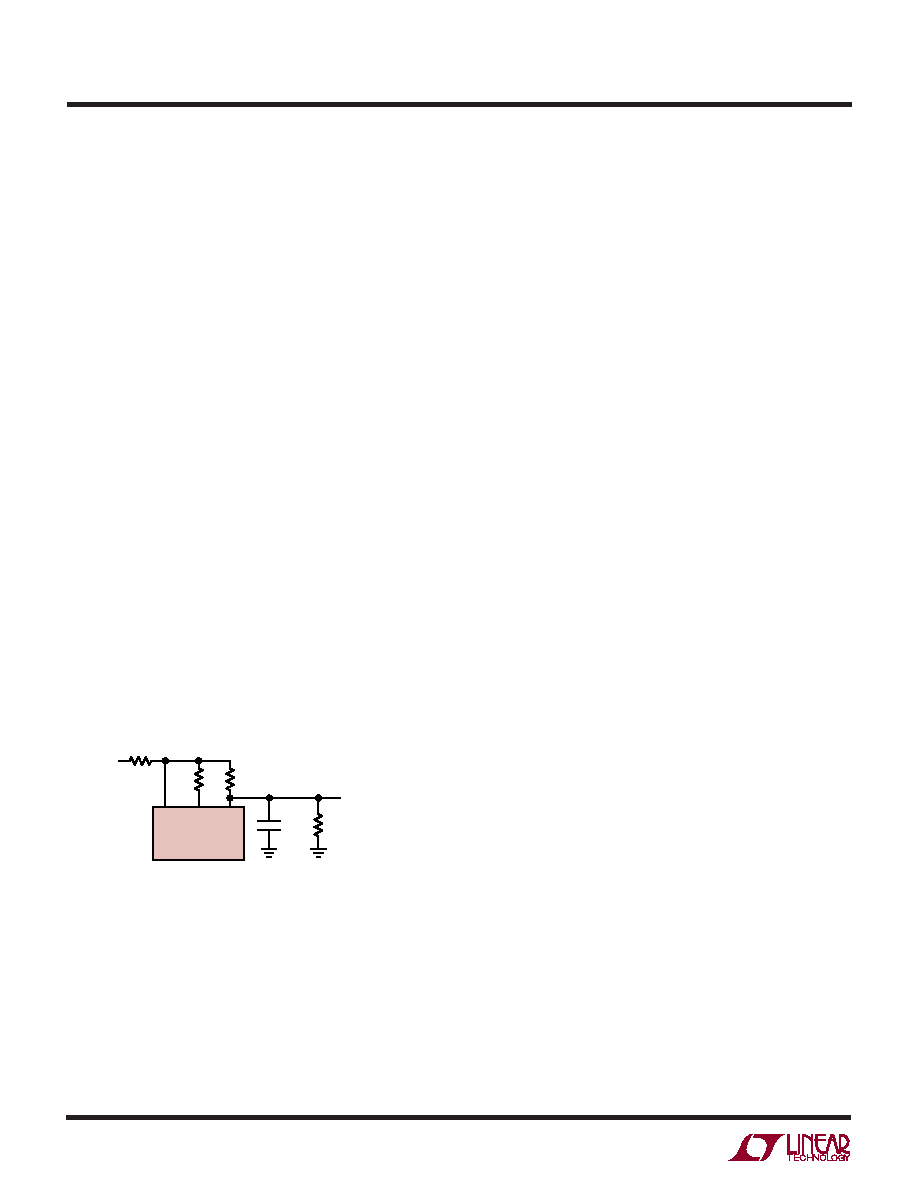
INV
V1
2nd ORDER
1/4 LTC1562-2
V2
1562-2 F08
R2
7.87k
CL
30pF
RL
(EXTERNAL
LOAD RESISTANCE)
RQ
5.49k
RIN
7.87k
VIN
VOUT
Figure 8. 200kHz, Q = 0.7 Lowpass Circuit
for Distortion vs Loading Test
Low Level or Wide Range Input Signals
The LTC1562-2 contains a built-in capability for low noise
amplification of low level signals. The ZIN impedance in
each 2nd order section controls the block’s gain. When set
for unity passband gain, a 2nd order section can deliver an
output signal 99dB above the noise level. If low level inputs
相关PDF资料 |
PDF描述 |
|---|---|
| VE-JWK-IW-B1 | CONVERTER MOD DC/DC 40V 100W |
| LTC1562CG#PBF | IC FILTER UNIV RC QUAD LN 20SSOP |
| VE-JWJ-IW-B1 | CONVERTER MOD DC/DC 36V 100W |
| LTC1564CG#PBF | IC ANTIALIASING FILTER 16-SSOP |
| LTC6603IUF#PBF | IC FILTER LOWPASS 24-QFN |
相关代理商/技术参数 |
参数描述 |
|---|---|
| LTC1562CGPBF | 制造商:Linear Technology 功能描述:Active Filter Quad 8th Order 150kHz SSOP |
| LTC1562CN | 功能描述:IC FILTER UNIV RC QUAD LN 16DIP RoHS:否 类别:集成电路 (IC) >> 接口 - 滤波器 - 有源 系列:- 产品培训模块:Lead (SnPb) Finish for COTS Obsolescence Mitigation Program 标准包装:1,000 系列:- 滤波器类型:连续时间,带通低通 频率 - 截止或中心:150kHz 滤波器数:4 滤波器阶数:8th 电源电压:4.74 V ~ 11 V,±2.37 V ~ 5.5 V 安装类型:表面贴装 封装/外壳:28-SOIC(0.295",7.50mm 宽) 供应商设备封装:28-SOIC W 包装:带卷 (TR) |
| LTC1562CN#PBF | 功能描述:IC FILTER UNIV RC QUAD LN 16DIP RoHS:是 类别:集成电路 (IC) >> 接口 - 滤波器 - 有源 系列:- 产品培训模块:Lead (SnPb) Finish for COTS Obsolescence Mitigation Program 标准包装:1,000 系列:- 滤波器类型:连续时间,带通低通 频率 - 截止或中心:150kHz 滤波器数:4 滤波器阶数:8th 电源电压:4.74 V ~ 11 V,±2.37 V ~ 5.5 V 安装类型:表面贴装 封装/外壳:28-SOIC(0.295",7.50mm 宽) 供应商设备封装:28-SOIC W 包装:带卷 (TR) |
| LTC1562IG | 功能描述:IC FILTER UNIVRSL RC QUAD 20SSOP RoHS:否 类别:集成电路 (IC) >> 接口 - 滤波器 - 有源 系列:- 产品培训模块:Lead (SnPb) Finish for COTS Obsolescence Mitigation Program 标准包装:1,000 系列:- 滤波器类型:连续时间,带通低通 频率 - 截止或中心:150kHz 滤波器数:4 滤波器阶数:8th 电源电压:4.74 V ~ 11 V,±2.37 V ~ 5.5 V 安装类型:表面贴装 封装/外壳:28-SOIC(0.295",7.50mm 宽) 供应商设备封装:28-SOIC W 包装:带卷 (TR) |
| LTC1562IG#PBF | 功能描述:IC FILTER UNIV RC QUAD LN 20SSOP RoHS:是 类别:集成电路 (IC) >> 接口 - 滤波器 - 有源 系列:- 产品培训模块:Lead (SnPb) Finish for COTS Obsolescence Mitigation Program 标准包装:1,000 系列:- 滤波器类型:连续时间,带通低通 频率 - 截止或中心:150kHz 滤波器数:4 滤波器阶数:8th 电源电压:4.74 V ~ 11 V,±2.37 V ~ 5.5 V 安装类型:表面贴装 封装/外壳:28-SOIC(0.295",7.50mm 宽) 供应商设备封装:28-SOIC W 包装:带卷 (TR) |
发布紧急采购,3分钟左右您将得到回复。