参数资料
| 型号: | LTC1564IG#TR |
| 厂商: | Linear Technology |
| 文件页数: | 12/12页 |
| 文件大小: | 0K |
| 描述: | IC ANTIALIASING FILTER 16-SSOP |
| 标准包装: | 2,000 |
| 滤波器类型: | 抗混迭 |
| 频率 - 截止或中心: | 150kHz |
| 滤波器数: | 1 |
| 滤波器阶数: | 8th |
| 电源电压: | 2.7 V ~ 10.5 V |
| 安装类型: | 表面贴装 |
| 封装/外壳: | 16-SSOP(0.209",5.30mm 宽) |
| 供应商设备封装: | 16-SSOP |
| 包装: | 带卷 (TR) |
| 其它名称: | LTC1564IGTR |
9
LTC1564
1564fa
Functional Description
The LTC1564 is a self-contained, continuous time, vari-
able gain, high order analog lowpass filter. The gain
magnitude between IN and OUT pins is approximately
constant for signal frequency components up to the cutoff
frequency fC and falls off rapidly for frequencies above fC.
The pins IN, OUT and AGND (analog ground) are the sole
analog signal connections on the LTC1564; the others are
power supplies and digital control inputs to select fC (and
to select gain if desired). The fC range is 10kHz to 150kHz
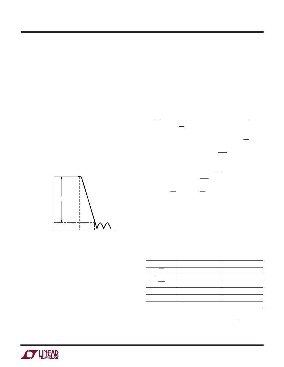
in 10kHz steps. The form of the lowpass frequency re-
sponse is an 8-pole elliptic type with two stopband notches
(Figure 4). This response rolls off by approximately 100dB
from fC to 2.5fC. The LTC1564 is laser trimmed for fC
accuracy, passband ripple, gain and offset. It delivers a
combination of 100+dB stopband attenuation, 100+dB
signal-to-noise ratio (SNR) and 100+kHz fC.
Digital Control
Logic levels for the LTC1564 digital inputs are nominally
rail-to-rail CMOS. (Logic 1 is V+, logic 0 is V– or alterna-
tively 0V with
±5V supplies). The part is tested with 10%
and 90% of full excursion on the inputs, thus
±1.08V at
±1.35V supplies, ±1.9V at ±2.375V and 0.5V and 4.5V at
±5V.
The fC and gain settings are always controlled by the out-
put of an on-chip CMOS latch. Inputs to this latch are the
pins F3 through F0, G3 through G0, the latch-enable con-
trol CS/HOLD and the asynchronous reset input RST. A
logic-0 input to CS/HOLD makes the latch transparent so
that the F and G input pins pass directly to the latch outputs
and therefore control the filter directly. Raising CS/HOLD
to logic 1 freezes the latch’s output so that the F and G input
pins have no effect. Logic 0 at the RST input at any time
resets the latch outputs to all zeros. The all-zero state, in
turn, imposes a mute mode with zero gain and low output
noise if the filter is powered on (EN = 0). The all-zeros
condition will persist until RST is returned to logic 1, non-
zero F and G inputs are set up and the latch outputs are
updated by CS/HOLD = 0. EN is a chip-enable input caus-
ing a shutdown state. Specific details on the digital con-
trols appear in the Pin Functions section of this data sheet.
Floatable Digital Inputs
Every digital input of the LTC1564 includes a small current
source (roughly 10
A) to float the CMOS input to V+ or V–
potential if the pin is unconnected. Table 4 summarizes the
open-circuit default levels.
Table 4. Open-Circuit Default Input Levels
INPUT
FLOATING LOGIC LEVEL
EFFECT
EN
1
Shutdown State
CS/HOLD
0
F and G Pins Enabled
RST
1
Latch Not Reset
F3 F2 F1 F0
0 0 1 0
fC = 20kHz
G3 G2 G1 G0
0 0 0 0
Unity Passband Gain
Note particularly that the pull-up current source at the EN
pin forces the LTC1564 to the shutdown state if this pin is
left open. Therefore the user
must connect EN deliberately
to a logic-0 level (V–, or optionally 0V with
±5V supplies)
for normal filter operation. The other digital inputs float to
APPLICATIO S I FOR ATIO
WU
UU
100dB
FREQUENCY (Hz)
GAIN
(dB)
fC
2.5fC
1564 F04
Figure 4. General Shape of Frequency Response
Figure 3 is a block diagram showing analog signal path,
digital control latch, and analog ground (AGND) circuitry.
A proprietary active-RC architecture filters the analog
signal. This architecture limits internal noise sources to
near the fundamental “kT/C” bounds for a filter of this
order and power consumption. The variable gain capability
at the input is an integral part of the filter, and allows
boosting of low level input signals with little increase in
output referred noise. This permits the input noise floor to
drop steadily with increasing gain, enhancing the SNR at
lower signal levels. Such a property is difficult to achieve
in practice by combining separate variable gain amplifier
and filter circuits.
相关PDF资料 |
PDF描述 |
|---|---|
| LTC1565-31IS8#TR | IC FILTR 7TH ORDER 650KHZ 8-SOIC |
| LTC1566-1IS8#TRPBF | IC FILTER LP 7ORDER 2.3MHZ 8SOIC |
| LTC1569IS8-6#TRPBF | IC FILTER 10TH ORDR LOWPASS8SOIC |
| LTC1569IS8-7#TRPBF | IC FILTER 10TH ORDR LOWPASS8SOIC |
| LTC1685IS8 | IC TXRX RS485 PREC DELAY 8-SOIC |
相关代理商/技术参数 |
参数描述 |
|---|---|
| LTC1565-31CS8 | 功能描述:IC FILTR 7TH ORDER 650KHZ 8-SOIC RoHS:否 类别:集成电路 (IC) >> 接口 - 滤波器 - 有源 系列:- 产品培训模块:Lead (SnPb) Finish for COTS Obsolescence Mitigation Program 标准包装:1,000 系列:- 滤波器类型:连续时间,带通低通 频率 - 截止或中心:150kHz 滤波器数:4 滤波器阶数:8th 电源电压:4.74 V ~ 11 V,±2.37 V ~ 5.5 V 安装类型:表面贴装 封装/外壳:28-SOIC(0.295",7.50mm 宽) 供应商设备封装:28-SOIC W 包装:带卷 (TR) |
| LTC1565-31CS8#PBF | 功能描述:IC FILTR 7TH ORDER 650KHZ 8-SOIC RoHS:是 类别:集成电路 (IC) >> 接口 - 滤波器 - 有源 系列:- 产品培训模块:Lead (SnPb) Finish for COTS Obsolescence Mitigation Program 标准包装:1,000 系列:- 滤波器类型:连续时间,带通低通 频率 - 截止或中心:150kHz 滤波器数:4 滤波器阶数:8th 电源电压:4.74 V ~ 11 V,±2.37 V ~ 5.5 V 安装类型:表面贴装 封装/外壳:28-SOIC(0.295",7.50mm 宽) 供应商设备封装:28-SOIC W 包装:带卷 (TR) |
| LTC1565-31CS8#TR | 功能描述:IC FILTR 7TH ORDER 650KHZ 8-SOIC RoHS:否 类别:集成电路 (IC) >> 接口 - 滤波器 - 有源 系列:- 产品培训模块:Lead (SnPb) Finish for COTS Obsolescence Mitigation Program 标准包装:1,000 系列:- 滤波器类型:连续时间,带通低通 频率 - 截止或中心:150kHz 滤波器数:4 滤波器阶数:8th 电源电压:4.74 V ~ 11 V,±2.37 V ~ 5.5 V 安装类型:表面贴装 封装/外壳:28-SOIC(0.295",7.50mm 宽) 供应商设备封装:28-SOIC W 包装:带卷 (TR) |
| LTC1565-31CS8#TRPBF | 功能描述:IC FILTR 7TH ORDER 650KHZ 8-SOIC RoHS:是 类别:集成电路 (IC) >> 接口 - 滤波器 - 有源 系列:- 产品培训模块:Lead (SnPb) Finish for COTS Obsolescence Mitigation Program 标准包装:1,000 系列:- 滤波器类型:连续时间,带通低通 频率 - 截止或中心:150kHz 滤波器数:4 滤波器阶数:8th 电源电压:4.74 V ~ 11 V,±2.37 V ~ 5.5 V 安装类型:表面贴装 封装/外壳:28-SOIC(0.295",7.50mm 宽) 供应商设备封装:28-SOIC W 包装:带卷 (TR) |
| LTC1565-31IS8 | 功能描述:IC FILTR 7TH ORDER 650KHZ 8-SOIC RoHS:否 类别:集成电路 (IC) >> 接口 - 滤波器 - 有源 系列:- 产品培训模块:Lead (SnPb) Finish for COTS Obsolescence Mitigation Program 标准包装:1,000 系列:- 滤波器类型:连续时间,带通低通 频率 - 截止或中心:150kHz 滤波器数:4 滤波器阶数:8th 电源电压:4.74 V ~ 11 V,±2.37 V ~ 5.5 V 安装类型:表面贴装 封装/外壳:28-SOIC(0.295",7.50mm 宽) 供应商设备封装:28-SOIC W 包装:带卷 (TR) |
发布紧急采购,3分钟左右您将得到回复。