- 您现在的位置:买卖IC网 > PDF目录1934 > LTC1569IS8-7#TRPBF (Linear Technology)IC FILTER 10TH ORDR LOWPASS8SOIC PDF资料下载
参数资料
| 型号: | LTC1569IS8-7#TRPBF |
| 厂商: | Linear Technology |
| 文件页数: | 8/12页 |
| 文件大小: | 0K |
| 描述: | IC FILTER 10TH ORDR LOWPASS8SOIC |
| 标准包装: | 2,500 |
| 滤波器类型: | 线性相位,低通开关电容器 |
| 频率 - 截止或中心: | 300kHz |
| 滤波器数: | 1 |
| 滤波器阶数: | 10th |
| 安装类型: | 表面贴装 |
| 封装/外壳: | 8-SOIC(0.154",3.90mm 宽) |
| 供应商设备封装: | 8-SOIC |
| 包装: | 带卷 (TR) |
5
LTC1569-7
PIN FUNCTIONS
UU
U
IN +/IN – (Pins 1, 2): Signals can be applied to either or
both input pins. The DC gain from IN + (Pin 1) to OUT
(Pin 8) is 1.0, and the DC gain from Pin 2 to Pin 8 is –1. The
input range, input resistance and output range are de-
scribed in the Applications Information section. Input
voltages which exceed the power supply voltages should
be avoided. Transients will not cause latchup if the current
into/out of the input pins is limited to 20mA.
GND (Pin 3): The GND pin is the reference voltage for the
filter and should be externally biased to 2V (1.11V) to
maximize the dynamic range of the filter in applications
using a single 5V (3V) supply. For single supply operation,
the GND pin should be bypassed with a quality 1
F
ceramic capacitor to V – (Pin 4). The impedance of the
circuit biasing the GND pin should be less than 2k
as the
GND pin generates a small amount of AC and DC current.
For dual supply operation, connect Pin 3 to a high quality
DC ground. A ground plane should be used. A poor ground
will increase DC offset, clock feedthrough, noise and
distortion.
V –/V + (Pins 4, 7): For 3V, 5V and
±5V applications a
quality 1
F ceramic bypass capacitor is required from V+
(Pin 7) to V – (Pin 4) to provide the transient energy for the
internal clock drivers. The bypass should be as close as
possible to the IC. In dual supply applications (Pin 3 is
grounded), an additional 0.1
F bypass from V+ (Pin 7) to
GND (Pin 3) and V – (Pin 4) to GND (Pin 3) is recom-
mended.
The maximum voltage difference between GND (Pin 3) and
V + (Pin 7) should not exceed 5.5V.
DIV/CLK (Pin 5): DIV/CLK serves two functions. When the
internal oscillator is enabled, DIV/CLK can be used to
engage an internal divider. The internal divider is set to 1:1
when DIV/CLK is shorted to V – (Pin 4). The internal divider
is set to 4:1 when DIV/CLK is allowed to float (a 100pF
bypass to V – is recommended). The internal divider is set
to 16:1 when DIV/CLK is shorted to V + (Pin 7). In the
divide-by-4 and divide-by-16 modes the power supply
current is reduced by typically 60%.
When the internal oscillator is disabled (RX shorted
to V –) DIV/CLK becomes an input pin for applying an
external clock signal. For proper filter operation, the clock
waveform should be a squarewave with a duty cycle as
close as possible to 50% and CMOS voltages levels (see
Electrical Characteristics section for voltage levels). DIV/
CLK pin voltages which exceed the power supply voltages
should be avoided. Transients will not cause latchup if the
fault current into/out of the DIV/CLK pin is limited to 40mA.
RX (Pin 6): Connecting an external resistor between the RX
pin and V + (Pin 7) enables the internal oscillator. The value
of the resistor determines the frequency of oscillation. The
maximum recommended resistor value is 40k and the
minimum is 3.8k/8k (single 5V/3V supply). The internal
oscillator is disabled by shorting the RX pin to V – (Pin 4).
(Please refer to the Applications Information section.)
OUT (Pin 8): Filter Output. This pin can drive 10k
and/or
40pF loads. For larger capacitive loads, an external 100
series resistor is recommended. The output pin can ex-
ceed the power supply voltages by up to
±2V without
latchup.
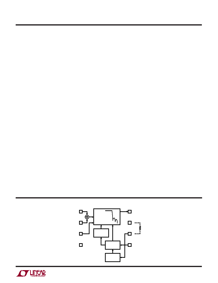
BLOCK DIAGRA
W
10TH ORDER
LINEAR PHASE
FILTER NETWORK
POWER
CONTROL
DIVIDER/
BUFFER
REXT
PRECISION
OSCILLATOR
5
6
7
8
4
3
2
1
OUT
V+
RX
DIV/CLK
IN+
IN–
GND
V–
1569-7 BD
相关PDF资料 |
PDF描述 |
|---|---|
| LTC1685IS8 | IC TXRX RS485 PREC DELAY 8-SOIC |
| LTC1755EGN#TR | IC SMART CARD INTERFACE 24SSOP |
| LTC1955IUH#TRPBF | IC SMART CARD INTERFACE DL 32QFN |
| LTC202CS#TRPBF | IC SWITCH QUAD SPST 16SOIC |
| LTC221CN#PBF | IC SWITCH QUAD SPST 16DIP |
相关代理商/技术参数 |
参数描述 |
|---|---|
| LTC1574CS | 功能描述:IC REG BUCK INV ADJ 16SOIC RoHS:否 类别:集成电路 (IC) >> PMIC - 稳压器 - DC DC 开关稳压器 系列:- 设计资源:Design Support Tool 标准包装:1 系列:- 类型:升压(升压) 输出类型:固定 输出数:1 输出电压:3V 输入电压:0.75 V ~ 2 V PWM 型:- 频率 - 开关:- 电流 - 输出:100mA 同步整流器:是 工作温度:-40°C ~ 85°C 安装类型:表面贴装 封装/外壳:SOT-23-5 细型,TSOT-23-5 包装:剪切带 (CT) 供应商设备封装:TSOT-23-5 其它名称:AS1323-BTTT-30CT |
| LTC1574CS#PBF | 功能描述:IC REG BUCK INV ADJ 16SOIC RoHS:是 类别:集成电路 (IC) >> PMIC - 稳压器 - DC DC 开关稳压器 系列:- 标准包装:250 系列:- 类型:降压(降压) 输出类型:固定 输出数:1 输出电压:1.2V 输入电压:2.05 V ~ 6 V PWM 型:电压模式 频率 - 开关:2MHz 电流 - 输出:500mA 同步整流器:是 工作温度:-40°C ~ 85°C 安装类型:表面贴装 封装/外壳:6-UFDFN 包装:带卷 (TR) 供应商设备封装:6-SON(1.45x1) 产品目录页面:1032 (CN2011-ZH PDF) 其它名称:296-25628-2 |
| LTC1574CS#TR | 功能描述:IC REG BUCK INV ADJ 16SOIC RoHS:否 类别:集成电路 (IC) >> PMIC - 稳压器 - DC DC 开关稳压器 系列:- 设计资源:Design Support Tool 标准包装:1 系列:- 类型:升压(升压) 输出类型:固定 输出数:1 输出电压:3V 输入电压:0.75 V ~ 2 V PWM 型:- 频率 - 开关:- 电流 - 输出:100mA 同步整流器:是 工作温度:-40°C ~ 85°C 安装类型:表面贴装 封装/外壳:SOT-23-5 细型,TSOT-23-5 包装:剪切带 (CT) 供应商设备封装:TSOT-23-5 其它名称:AS1323-BTTT-30CT |
| LTC1574CS#TRPBF | 功能描述:IC REG BUCK INV ADJ 16SOIC RoHS:是 类别:集成电路 (IC) >> PMIC - 稳压器 - DC DC 开关稳压器 系列:- 设计资源:Design Support Tool 标准包装:1 系列:- 类型:升压(升压) 输出类型:固定 输出数:1 输出电压:3V 输入电压:0.75 V ~ 2 V PWM 型:- 频率 - 开关:- 电流 - 输出:100mA 同步整流器:是 工作温度:-40°C ~ 85°C 安装类型:表面贴装 封装/外壳:SOT-23-5 细型,TSOT-23-5 包装:剪切带 (CT) 供应商设备封装:TSOT-23-5 其它名称:AS1323-BTTT-30CT |
| LTC1574CS-3.3 | 功能描述:IC REG BUCK INV 3.3V 16SOIC RoHS:否 类别:集成电路 (IC) >> PMIC - 稳压器 - DC DC 开关稳压器 系列:- 设计资源:Design Support Tool 标准包装:1 系列:- 类型:升压(升压) 输出类型:固定 输出数:1 输出电压:3V 输入电压:0.75 V ~ 2 V PWM 型:- 频率 - 开关:- 电流 - 输出:100mA 同步整流器:是 工作温度:-40°C ~ 85°C 安装类型:表面贴装 封装/外壳:SOT-23-5 细型,TSOT-23-5 包装:剪切带 (CT) 供应商设备封装:TSOT-23-5 其它名称:AS1323-BTTT-30CT |
发布紧急采购,3分钟左右您将得到回复。