- 您现在的位置:买卖IC网 > PDF目录10181 > LTC1608CG (Linear Technology)IC A/D CONV 16BIT SAMPLNG 36SSOP PDF资料下载
参数资料
| 型号: | LTC1608CG |
| 厂商: | Linear Technology |
| 文件页数: | 20/20页 |
| 文件大小: | 0K |
| 描述: | IC A/D CONV 16BIT SAMPLNG 36SSOP |
| 标准包装: | 37 |
| 位数: | 16 |
| 采样率(每秒): | 500k |
| 数据接口: | 并联 |
| 转换器数目: | 1 |
| 功率耗散(最大): | 420mW |
| 电压电源: | 模拟和数字,双 ± |
| 工作温度: | 0°C ~ 70°C |
| 安装类型: | 表面贴装 |
| 封装/外壳: | 36-SSOP(0.209",5.30mm 宽) |
| 供应商设备封装: | 36-SSOP |
| 包装: | 管件 |
| 输入数目和类型: | 2 个单端,双极;1 个差分,双极 |
| 其它名称: | Q917092 |
9
LTC1608
Timing and Control
Conversion start and data read operations are controlled
by three digital inputs: CONVST, CS and RD. A falling edge
applied to the CONVST pin will start a conversion after the
ADC has been selected (i.e., CS is low). Once initiated, it
cannot be restarted until the conversion is complete.
Converter status is indicated by the BUSY output. BUSY is
low during a conversion.
We recommend using a narrow logic low or narrow logic
high CONVST pulse to start a conversion as shown in
Figures 5 and 6. A narrow low or high CONVST pulse
prevents the rising edge of the CONVST pulse from upset-
ting the critical bit decisions during the conversion time.
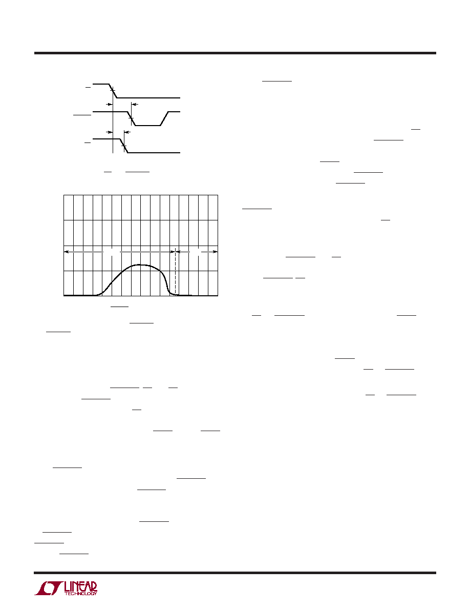
Figure 4 shows the change of the differential nonlinearity
error versus the low time of the CONVST pulse. As shown,
if CONVST returns high early in the conversion (e.g.,
CONVST low time <300ns), accuracy is unaffected. Simi-
larly, if CONVST returns high after the conversion is over
t2
t1
CS
CONVST
RD
1608 F03
Figure 3. CS top CONVST Setup Timing
Figure 4. Change in DNL vs CONVST Low Time. Be Sure the
CONVST Pulse Returns High Early in the Conversion or After
the End of Conversion
0
CHANGE
IN
DNL
(LSB)
1750
2000
1608 F04
250
500
1000
750
1250
1500
4
3
2
1
0
CONVST LOW TIME, t5 (ns)
tCONV
tACQ
APPLICATIO S I FOR ATIO
WU
UU
(e.g., CONVST low time >tCONV), accuracy is unaffected.
For best results, keep t5 less than 500ns or greater than
tCONV.
Figures 5 through 9 show several different modes of
operation. In modes 1a and 1b (Figures 5 and 6), CS and
RD are both tied low. The falling edge of CONVST starts the
conversion. The data outputs are always enabled and data
can be latched with the BUSY rising edge. Mode 1a shows
operation with a narrow logic low CONVST pulse. Mode 1b
shows a narrow logic high CONVST pulse.
In mode 2 (Figure 7) CS is tied low. The falling edge of
CONVST signal starts the conversion. Data outputs are in
three-state until read by the MPU with the RD signal. Mode
2 can be used for operation with a shared data bus.
In slow memory and ROM modes (Figures 8 and 9), CS is
tied low and CONVST and RD are tied together. The MPU
starts the conversion and reads the output with the com-
bined CONVST-RD signal. Conversions are started by the
MPU or DSP (no external sample clock is needed).
In slow memory mode, the processor applies a logic low
to RD (= CONVST), starting the conversion. BUSY goes
low, forcing the processor into a wait state. The previous
conversion result appears on the data outputs. When the
conversion is complete, the new conversion results
appear on the data outputs; BUSY goes high, releasing the
processor and the processor takes RD (= CONVST) back
high and reads the new conversion data.
In ROM mode, the processor takes RD (= CONVST) low,
starting a conversion and reading the previous conversion
result. After the conversion is complete, the processor can
read the new result and initiate another conversion.
DIFFERENTIAL ANALOG INPUTS
Driving the Analog Inputs
The differential analog inputs of the LTC1608 are easy to
drive. The inputs may be driven differentially or as a single-
ended input (i.e., the AIN– input is grounded). The AIN+ and
AIN– inputs are sampled at the same instant. Any un-
wanted signal that is common mode to both inputs will be
reduced by the common mode rejection of the sample-
and-hold circuit. The inputs draw only one small current
相关PDF资料 |
PDF描述 |
|---|---|
| MS27473E18B35P | CONN PLUG 66POS STRAIGHT W/PINS |
| VE-B7H-MY | CONVERTER MOD DC/DC 52V 50W |
| LTC2850CS8#TRPBF | IC TXRX RS485 20MBPS 8-SOIC |
| VE-B74-MY | CONVERTER MOD DC/DC 48V 50W |
| MS27472T18F11S | CONN RCPT 11POS WALL MT W/SCKT |
相关代理商/技术参数 |
参数描述 |
|---|---|
| LTC1608CG#PBF | 功能描述:IC A/D CONV 16BIT SAMPLNG 36SSOP RoHS:是 类别:集成电路 (IC) >> 数据采集 - 模数转换器 系列:- 标准包装:1 系列:microPOWER™ 位数:8 采样率(每秒):1M 数据接口:串行,SPI? 转换器数目:1 功率耗散(最大):- 电压电源:模拟和数字 工作温度:-40°C ~ 125°C 安装类型:表面贴装 封装/外壳:24-VFQFN 裸露焊盘 供应商设备封装:24-VQFN 裸露焊盘(4x4) 包装:Digi-Reel® 输入数目和类型:8 个单端,单极 产品目录页面:892 (CN2011-ZH PDF) 其它名称:296-25851-6 |
| LTC1608CG#TR | 功能描述:IC ADC 16BIT 5V SAMPLING 36SSOP RoHS:否 类别:集成电路 (IC) >> 数据采集 - 模数转换器 系列:- 标准包装:1,000 系列:- 位数:12 采样率(每秒):300k 数据接口:并联 转换器数目:1 功率耗散(最大):75mW 电压电源:单电源 工作温度:0°C ~ 70°C 安装类型:表面贴装 封装/外壳:24-SOIC(0.295",7.50mm 宽) 供应商设备封装:24-SOIC 包装:带卷 (TR) 输入数目和类型:1 个单端,单极;1 个单端,双极 |
| LTC1608CG#TRPBF | 功能描述:IC A/D CONV 16BIT SAMPLNG 36SSOP RoHS:是 类别:集成电路 (IC) >> 数据采集 - 模数转换器 系列:- 标准包装:1,000 系列:- 位数:12 采样率(每秒):300k 数据接口:并联 转换器数目:1 功率耗散(最大):75mW 电压电源:单电源 工作温度:0°C ~ 70°C 安装类型:表面贴装 封装/外壳:24-SOIC(0.295",7.50mm 宽) 供应商设备封装:24-SOIC 包装:带卷 (TR) 输入数目和类型:1 个单端,单极;1 个单端,双极 |
| LTC1608IG | 功能描述:IC CONV A/D 16BIT 500KSPS 36SSOP RoHS:否 类别:集成电路 (IC) >> 数据采集 - 模数转换器 系列:- 标准包装:1 系列:- 位数:14 采样率(每秒):83k 数据接口:串行,并联 转换器数目:1 功率耗散(最大):95mW 电压电源:双 ± 工作温度:0°C ~ 70°C 安装类型:通孔 封装/外壳:28-DIP(0.600",15.24mm) 供应商设备封装:28-PDIP 包装:管件 输入数目和类型:1 个单端,双极 |
| LTC1608IG#PBF | 功能描述:IC A/D CONV 16BIT SAMPLNG 36SSOP RoHS:是 类别:集成电路 (IC) >> 数据采集 - 模数转换器 系列:- 其它有关文件:TSA1204 View All Specifications 标准包装:1 系列:- 位数:12 采样率(每秒):20M 数据接口:并联 转换器数目:2 功率耗散(最大):155mW 电压电源:模拟和数字 工作温度:-40°C ~ 85°C 安装类型:表面贴装 封装/外壳:48-TQFP 供应商设备封装:48-TQFP(7x7) 包装:Digi-Reel® 输入数目和类型:4 个单端,单极;2 个差分,单极 产品目录页面:1156 (CN2011-ZH PDF) 其它名称:497-5435-6 |
发布紧急采购,3分钟左右您将得到回复。