- 您现在的位置:买卖IC网 > PDF目录10181 > LTC1608CG (Linear Technology)IC A/D CONV 16BIT SAMPLNG 36SSOP PDF资料下载
参数资料
| 型号: | LTC1608CG |
| 厂商: | Linear Technology |
| 文件页数: | 6/20页 |
| 文件大小: | 0K |
| 描述: | IC A/D CONV 16BIT SAMPLNG 36SSOP |
| 标准包装: | 37 |
| 位数: | 16 |
| 采样率(每秒): | 500k |
| 数据接口: | 并联 |
| 转换器数目: | 1 |
| 功率耗散(最大): | 420mW |
| 电压电源: | 模拟和数字,双 ± |
| 工作温度: | 0°C ~ 70°C |
| 安装类型: | 表面贴装 |
| 封装/外壳: | 36-SSOP(0.209",5.30mm 宽) |
| 供应商设备封装: | 36-SSOP |
| 包装: | 管件 |
| 输入数目和类型: | 2 个单端,双极;1 个差分,双极 |
| 其它名称: | Q917092 |
14
LTC1608
APPLICATIO S I FOR ATIO
WU
UU
LTC1608
AIN
+
AIN
–
VREF
0V TO
5V
±2.5V
REFCOMP
AGND
1608 F14b
1
2
3
4
5
22
F
ANALOG INPUT
–
+
Figure 14b. Selectable 0V to 5V or
±2.5V Input Range
Differential inputs allow greater flexibility for accepting
different input ranges. Figure 14b shows a circuit that
converts a 0V to 5V analog input signal with only an
additional buffer that is not in the signal path.
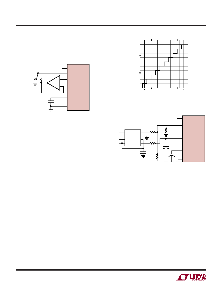
Full-Scale and Offset Adjustment
Figure 15a shows the ideal input/output characteristics
for the LTC1608. The code transitions occur midway
between successive integer LSB values (i.e., – FS +
0.5LSB, – FS + 1.5LSB, – FS + 2.5LSB,... FS – 1.5LSB,
FS – 0.5LSB). The output is two’s complement binary with
1LSB = FS – (– FS)/65536 = 5V/65536 = 76.3
V.
In applications where absolute accuracy is important,
offset and full-scale errors can be adjusted to zero. Offset
error must be adjusted before full-scale error. Figure 15b
shows the extra components required for full-scale error
adjustment. Zero offset is achieved by adjusting the offset
applied to the AIN– input. For zero offset error, apply
–38
V (i.e., –0.5LSB) at AIN+ and adjust the offset at the
AIN– input by varying the output voltage of pin VOUTA from
the LTC1662 until the output code flickers between 0000
0000 0000 0000 and 1111 1111 1111 1111. For full-scale
adjustment, an input voltage of 2.499886V (FS/2 – 1.5LSBs)
is applied to AIN+ and the output voltage of pin VOUTB is
adjusted until the output code flickers between 0111 1111
1111 1110 and 0111 1111 1111 1111.
BOARD LAYOUT AND GROUNDING
Wire wrap boards are not recommended for high resolu-
tion or high speed A/D converters. To obtain the best per-
formance from the LTC1608, a printed circuit board with
ANALOG
INPUT
1608 F15b
1
2
3
80.6k
1%
OFFSET ADJ RANGE:
±0.125%
FULL-SCALE ADJ RANGE:
±0.25%
R1
40.2k
4
5
0.1
F
5V
22
F
–5V
R3
1.5M
R2
100
+
2.2
F
+
AIN
+
AIN
–
VREF
REFCOMP
AGND
LTC1608
LTC1662
CS/LD
SCK
SDI
REF
VOUTA
GND
VCC
VOUTB
Figure 15b. Offset and Full-Scale Adjust Circuit
1608 F15a
011...111
011...110
000...001
000...000
111...111
111...110
100...001
100...000
FS – 1LSB
– (FS – 1LSB)
INPUT VOLTAGE (AIN
+ – A
IN
–)
OUTPUT
CODE
Figure 15a. LTC1608 Transfer Characteristics
ground plane is required. Layout should ensure that digital
and analog signal lines are separated as much as possible.
Particular care should be taken not to run any digital track
alongside an analog signal track or underneath the ADC.The
analog input should be screened by AGND.
An analog ground plane separate from the logic system
ground should be established under and around the ADC.
Pin 5 to Pin 8 (AGNDs), Pin 10 (ADC’s DGND) and all other
analog grounds should be connected to this single analog
ground point. The REFCOMP bypass capacitor and the
DVDD bypass capacitor should also be connected to this
analog ground plane. No other digital grounds should be
connected to this analog ground plane. Low impedance
analog and digital power supply common returns are
essential to low noise operation of the ADC and the foil
width for these tracks should be as wide as possible. In
相关PDF资料 |
PDF描述 |
|---|---|
| MS27473E18B35P | CONN PLUG 66POS STRAIGHT W/PINS |
| VE-B7H-MY | CONVERTER MOD DC/DC 52V 50W |
| LTC2850CS8#TRPBF | IC TXRX RS485 20MBPS 8-SOIC |
| VE-B74-MY | CONVERTER MOD DC/DC 48V 50W |
| MS27472T18F11S | CONN RCPT 11POS WALL MT W/SCKT |
相关代理商/技术参数 |
参数描述 |
|---|---|
| LTC1608CG#PBF | 功能描述:IC A/D CONV 16BIT SAMPLNG 36SSOP RoHS:是 类别:集成电路 (IC) >> 数据采集 - 模数转换器 系列:- 标准包装:1 系列:microPOWER™ 位数:8 采样率(每秒):1M 数据接口:串行,SPI? 转换器数目:1 功率耗散(最大):- 电压电源:模拟和数字 工作温度:-40°C ~ 125°C 安装类型:表面贴装 封装/外壳:24-VFQFN 裸露焊盘 供应商设备封装:24-VQFN 裸露焊盘(4x4) 包装:Digi-Reel® 输入数目和类型:8 个单端,单极 产品目录页面:892 (CN2011-ZH PDF) 其它名称:296-25851-6 |
| LTC1608CG#TR | 功能描述:IC ADC 16BIT 5V SAMPLING 36SSOP RoHS:否 类别:集成电路 (IC) >> 数据采集 - 模数转换器 系列:- 标准包装:1,000 系列:- 位数:12 采样率(每秒):300k 数据接口:并联 转换器数目:1 功率耗散(最大):75mW 电压电源:单电源 工作温度:0°C ~ 70°C 安装类型:表面贴装 封装/外壳:24-SOIC(0.295",7.50mm 宽) 供应商设备封装:24-SOIC 包装:带卷 (TR) 输入数目和类型:1 个单端,单极;1 个单端,双极 |
| LTC1608CG#TRPBF | 功能描述:IC A/D CONV 16BIT SAMPLNG 36SSOP RoHS:是 类别:集成电路 (IC) >> 数据采集 - 模数转换器 系列:- 标准包装:1,000 系列:- 位数:12 采样率(每秒):300k 数据接口:并联 转换器数目:1 功率耗散(最大):75mW 电压电源:单电源 工作温度:0°C ~ 70°C 安装类型:表面贴装 封装/外壳:24-SOIC(0.295",7.50mm 宽) 供应商设备封装:24-SOIC 包装:带卷 (TR) 输入数目和类型:1 个单端,单极;1 个单端,双极 |
| LTC1608IG | 功能描述:IC CONV A/D 16BIT 500KSPS 36SSOP RoHS:否 类别:集成电路 (IC) >> 数据采集 - 模数转换器 系列:- 标准包装:1 系列:- 位数:14 采样率(每秒):83k 数据接口:串行,并联 转换器数目:1 功率耗散(最大):95mW 电压电源:双 ± 工作温度:0°C ~ 70°C 安装类型:通孔 封装/外壳:28-DIP(0.600",15.24mm) 供应商设备封装:28-PDIP 包装:管件 输入数目和类型:1 个单端,双极 |
| LTC1608IG#PBF | 功能描述:IC A/D CONV 16BIT SAMPLNG 36SSOP RoHS:是 类别:集成电路 (IC) >> 数据采集 - 模数转换器 系列:- 其它有关文件:TSA1204 View All Specifications 标准包装:1 系列:- 位数:12 采样率(每秒):20M 数据接口:并联 转换器数目:2 功率耗散(最大):155mW 电压电源:模拟和数字 工作温度:-40°C ~ 85°C 安装类型:表面贴装 封装/外壳:48-TQFP 供应商设备封装:48-TQFP(7x7) 包装:Digi-Reel® 输入数目和类型:4 个单端,单极;2 个差分,单极 产品目录页面:1156 (CN2011-ZH PDF) 其它名称:497-5435-6 |
发布紧急采购,3分钟左右您将得到回复。