- 您现在的位置:买卖IC网 > PDF目录15263 > LTC1628CUH#TR (Linear Technology)IC REG CTRLR BUCK PWM CM 32-QFN PDF资料下载
参数资料
| 型号: | LTC1628CUH#TR |
| 厂商: | Linear Technology |
| 文件页数: | 18/32页 |
| 文件大小: | 0K |
| 描述: | IC REG CTRLR BUCK PWM CM 32-QFN |
| 标准包装: | 2,500 |
| PWM 型: | 电流模式 |
| 输出数: | 2 |
| 频率 - 最大: | 360kHz |
| 占空比: | 99.4% |
| 电源电压: | 3.5 V ~ 30 V |
| 降压: | 是 |
| 升压: | 无 |
| 回扫: | 无 |
| 反相: | 无 |
| 倍增器: | 无 |
| 除法器: | 无 |
| Cuk: | 无 |
| 隔离: | 无 |
| 工作温度: | 0°C ~ 85°C |
| 封装/外壳: | 32-WFQFN 裸露焊盘 |
| 包装: | 带卷 (TR) |
| 其它名称: | LTC1628CUHTR |
第1页第2页第3页第4页第5页第6页第7页第8页第9页第10页第11页第12页第13页第14页第15页第16页第17页当前第18页第19页第20页第21页第22页第23页第24页第25页第26页第27页第28页第29页第30页第31页第32页
�� �
�
�LTC1628/LTC1628-PG�
�APPLICATIO� S� I� FOR� ATIO�
�derived� from� the� output� during� normal� operation� (4.7V� <�
�V� OUT� <� 7V)� and� from� the� internal� regulator� when� the� output�
�is� out� of� regulation� (start-up,� short-circuit).� If� more� cur-�
�rent� is� required� through� the� EXTV� CC� switch� than� is� speci-�
�fied,� an� external� Schottky� diode� can� be� added� between� the�
�EXTV� CC� and� INTV� CC� pins.� Do� not� apply� greater� than� 7V� to�
�the� EXTV� CC� pin� and� ensure� that� EXTV� CC� <� V� IN� .�
�Significant� efficiency� gains� can� be� realized� by� powering�
�INTV� CC� from� the� output,� since� the� V� IN� current� resulting�
�from� the� driver� and� control� currents� will� be� scaled� by� a�
�factor� of� (Duty� Cycle)/(Efficiency).� For� 5V� regulators� this�
�supply� means� connecting� the� EXTV� CC� pin� directly� to� V� OUT� .�
�However,� for� 3.3V� and� other� lower� voltage� regulators,�
�additional� circuitry� is� required� to� derive� INTV� CC� power�
�from� the� output.�
�The� following� list� summarizes� the� four� possible� connec-�
�tions� for� EXTV� CC:�
�1.� EXTV� CC� Left� Open� (or� Grounded).� This� will� cause� INTV� CC�
�to� be� powered� from� the� internal� 5V� regulator� resulting� in�
�an� efficiency� penalty� of� up� to� 10%� at� high� input� voltages.�
�2.� EXTV� CC� Connected� directly� to� V� OUT� .� This� is� the� normal�
�connection� for� a� 5V� regulator� and� provides� the� highest�
�efficiency.�
�3.� EXTV� CC� Connected� to� an� External� supply.� If� an� external�
�supply� is� available� in� the� 5V� to� 7V� range,� it� may� be� used� to�
�power� EXTV� CC� providing� it� is� compatible� with� the� MOSFET�
�gate� drive� requirements.�
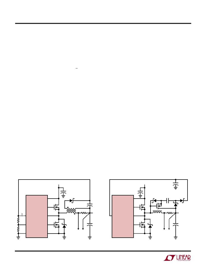
�4.� EXTV� CC� Connected� to� an� Output-Derived� Boost� Net-�
�work.� For� 3.3V� and� other� low� voltage� regulators,� efficiency�
�gains� can� still� be� realized� by� connecting� EXTV� CC� to� an�
�output-derived� voltage� that� has� been� boosted� to� greater�
�than� 4.7V.� This� can� be� done� with� either� the� inductive� boost�
�winding� as� shown� in� Figure� 6a� or� the� capacitive� charge�
�pump� shown� in� Figure� 6b.� The� charge� pump� has� the�
�advantage� of� simple� magnetics.�
�Topside� MOSFET� Driver� Supply� (C� B� ,� D� B� )�
�External� bootstrap� capacitors� C� B� connected� to� the� BOOST�
�pins� supply� the� gate� drive� voltages� for� the� topside� MOSFETs.�
�Capacitor� C� B� in� the� functional� diagram� is� charged� though�
�external� diode� D� B� from� INTV� CC� when� the� SW� pin� is� low.�
�When� one� of� the� topside� MOSFETs� is� to� be� turned� on,� the�
�driver� places� the� C� B� voltage� across� the� gate-source� of� the�
�desired� MOSFET.� This� enhances� the� MOSFET� and� turns� on�
�the� topside� switch.� The� switch� node� voltage,� SW,� rises� to�
�V� IN� and� the� BOOST� pin� follows.� With� the� topside� MOSFET�
�on,� the� boost� voltage� is� above� the� input� supply:� V� BOOST� =�
�V� IN� +� V� INTVCC� .� The� value� of� the� boost� capacitor� C� B� needs�
�to� be� 100� times� that� of� the� total� input� capacitance� of� the�
�topside� MOSFET(s).� The� reverse� breakdown� of� the� exter-�
�nal� Schottky� diode� must� be� greater� than� V� IN(MAX)� .� When�
�adjusting� the� gate� drive� level,� the� final� arbiter� is� the� total�
�input� current� for� the� regulator.� If� a� change� is� made� and� the�
�input� current� decreases,� then� the� efficiency� has� improved.�
�If� there� is� no� change� in� input� current,� then� there� is� no�
�change� in� efficiency.�
�OPTIONAL� EXTV� CC�
�V� IN�
�V� IN�
�+�
�1� μ� F�
�CONNECTION�
�5V� <� V� SEC� <� 7V�
�+�
�C� IN�
�C� IN�
�+�
�V� IN�
�V� SEC�
�V� IN�
�BAT85�
�0.22� μ� F�
�BAT85�
�LTC1628�
�TG1�
�N-CH�
�+�
�1� μ� F�
�LTC1628�
�TG1�
�N-CH�
�VN2222LL�
�BAT85�
�R� SENSE�
�V� OUT�
�R� SENSE�
�V� OUT�
�R6�
�EXTV� CC�
�SW�
�T1�
�1:N�
�+�
�EXTV� CC�
�SW�
�L1�
�+�
�R5�
�FCB�
�SGND�
�BG1�
�PGND�
�N-CH�
�C� OUT�
�BG1�
�PGND�
�N-CH�
�C� OUT�
�1628� F06a�
�Figure� 6a.� Secondary� Output� Loop� &� EXTV� CC� Connection�
�1628� F06b�
�Figure� 6b.� Capacitive� Charge� Pump� for� EXTV� CC�
�1628fb�
�18�
�相关PDF资料 |
PDF描述 |
|---|---|
| H2BXG-10108-V8-ND | JUMPER-H1501TR/A3048V/X 8" |
| LTC3723EGN-1#TRPBF | IC REG CTRLR FLYBK ISO CM 16SSOP |
| LTC3723EGN-1#TR | IC REG CTRLR FLYBK ISO CM 16SSOP |
| LTC3723EGN-2#TRPBF | IC REG CTRLR FLYBK ISO VM 16SSOP |
| H2BXG-10108-S8-ND | JUMPER-H1501TR/A3048S/X 8" |
相关代理商/技术参数 |
参数描述 |
|---|---|
| LTC1628IG | 功能描述:IC REG CTRLR BUCK PWM CM 28-SSOP RoHS:否 类别:集成电路 (IC) >> PMIC - 稳压器 - DC DC 切换控制器 系列:- 标准包装:4,500 系列:PowerWise® PWM 型:控制器 输出数:1 频率 - 最大:1MHz 占空比:95% 电源电压:2.8 V ~ 5.5 V 降压:是 升压:无 回扫:无 反相:无 倍增器:无 除法器:无 Cuk:无 隔离:无 工作温度:-40°C ~ 125°C 封装/外壳:6-WDFN 裸露焊盘 包装:带卷 (TR) 配用:LM1771EVAL-ND - BOARD EVALUATION LM1771 其它名称:LM1771SSDX |
| LTC1628IG#PBF | 功能描述:IC REG CTRLR BUCK PWM CM 28-SSOP RoHS:是 类别:集成电路 (IC) >> PMIC - 稳压器 - DC DC 切换控制器 系列:- 特色产品:LM3753/54 Scalable 2-Phase Synchronous Buck Controllers 标准包装:1 系列:PowerWise® PWM 型:电压模式 输出数:1 频率 - 最大:1MHz 占空比:81% 电源电压:4.5 V ~ 18 V 降压:是 升压:无 回扫:无 反相:无 倍增器:无 除法器:无 Cuk:无 隔离:无 工作温度:-5°C ~ 125°C 封装/外壳:32-WFQFN 裸露焊盘 包装:Digi-Reel® 产品目录页面:1303 (CN2011-ZH PDF) 其它名称:LM3754SQDKR |
| LTC1628IG#TR | 功能描述:IC REG CTRLR BUCK PWM CM 28-SSOP RoHS:否 类别:集成电路 (IC) >> PMIC - 稳压器 - DC DC 切换控制器 系列:- 标准包装:4,500 系列:PowerWise® PWM 型:控制器 输出数:1 频率 - 最大:1MHz 占空比:95% 电源电压:2.8 V ~ 5.5 V 降压:是 升压:无 回扫:无 反相:无 倍增器:无 除法器:无 Cuk:无 隔离:无 工作温度:-40°C ~ 125°C 封装/外壳:6-WDFN 裸露焊盘 包装:带卷 (TR) 配用:LM1771EVAL-ND - BOARD EVALUATION LM1771 其它名称:LM1771SSDX |
| LTC1628IG#TRPBF | 功能描述:IC REG CTRLR BUCK PWM CM 28-SSOP RoHS:是 类别:集成电路 (IC) >> PMIC - 稳压器 - DC DC 切换控制器 系列:- 标准包装:4,500 系列:PowerWise® PWM 型:控制器 输出数:1 频率 - 最大:1MHz 占空比:95% 电源电压:2.8 V ~ 5.5 V 降压:是 升压:无 回扫:无 反相:无 倍增器:无 除法器:无 Cuk:无 隔离:无 工作温度:-40°C ~ 125°C 封装/外壳:6-WDFN 裸露焊盘 包装:带卷 (TR) 配用:LM1771EVAL-ND - BOARD EVALUATION LM1771 其它名称:LM1771SSDX |
| LTC1628IGPBF | 制造商:Linear Technology 功能描述:DC-DC Controller Dual Step-Dn 36V SSOP28 |
发布紧急采购,3分钟左右您将得到回复。