- 您现在的位置:买卖IC网 > PDF目录15241 > LTC1649CS (Linear Technology)IC REG CTRLR BUCK PWM VM 16-SOIC PDF资料下载
参数资料
| 型号: | LTC1649CS |
| 厂商: | Linear Technology |
| 文件页数: | 12/16页 |
| 文件大小: | 0K |
| 描述: | IC REG CTRLR BUCK PWM VM 16-SOIC |
| 标准包装: | 50 |
| PWM 型: | 电压模式 |
| 输出数: | 1 |
| 频率 - 最大: | 260kHz |
| 占空比: | 93% |
| 电源电压: | 2.7 V ~ 5 V |
| 降压: | 是 |
| 升压: | 无 |
| 回扫: | 无 |
| 反相: | 无 |
| 倍增器: | 无 |
| 除法器: | 无 |
| Cuk: | 无 |
| 隔离: | 无 |
| 工作温度: | 0°C ~ 70°C |
| 封装/外壳: | 16-SOIC(0.154",3.90mm 宽) |
| 包装: | 管件 |
| 产品目录页面: | 1333 (CN2011-ZH PDF) |
�� �
�
�LTC1649�
�APPLICATIO� N� S� I� N� FOR� M� ATIO� N�
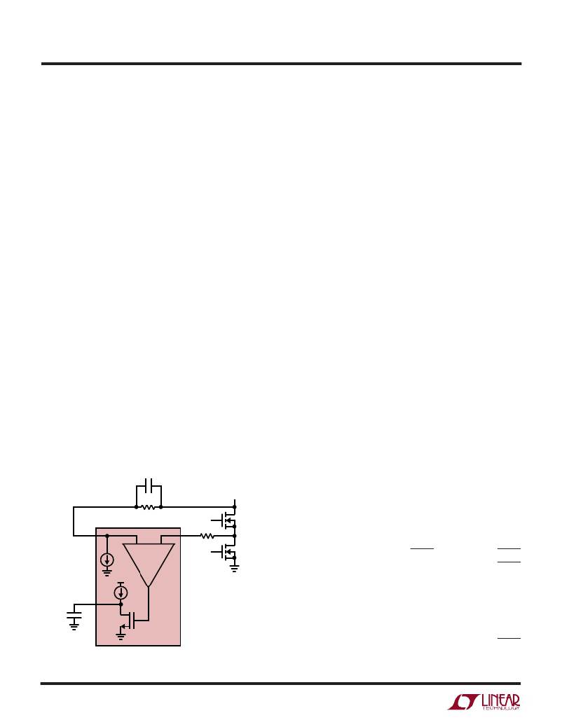
�The� LTC1649� detects� the� output� current� by� watching� the�
�voltage� at� I� FB� while� Q1� is� ON.� The� I� LIM� amplifier� compares�
�this� voltage� to� the� voltage� at� I� MAX� (Figure� 7).� In� the� ON�
�state,� Q1� has� a� known� resistance;� by� calculating� back-�
�wards,� the� voltage� generated� at� I� FB� by� the� maximum�
�output� current� in� Q1� can� be� determined.� As� I� FB� falls� below�
�I� MAX� ,� I� LIM� will� begin� to� sink� current� from� the� soft� start� pin,�
�causing� the� voltage� at� SS� to� fall.� As� SS� falls,� it� will� limit� the�
�output� duty� cycle,� limiting� the� current� at� the� output.�
�Eventually� the� system� will� reach� equilibrium,� where� the�
�pull-up� current� at� the� SS� pin� matches� the� pull-down�
�current� in� the� I� LIM� amplifier;� the� LTC1649� will� stay� in� this�
�state� until� the� overcurrent� condition� disappears.� At� this�
�time� I� FB� will� rise,� I� LIM� will� stop� sinking� current� and� the�
�internal� pull-up� will� recharge� the� soft� start� capacitor,�
�restoring� normal� operation.� Note� that� the� I� FB� pin� requires�
�an� external� 1k� series� resistor� to� prevent� voltage� transients�
�at� the� drain� of� Q2� from� damaging� internal� structures.�
�The� I� LIM� amplifier� pulls� current� out� of� SS� in� proportion� to�
�the� difference� between� I� FB� and� I� MAX� .� Under� mild� overload�
�conditions,� the� SS� pin� will� fall� gradually,� creating� a� time�
�delay� before� current� limit� takes� effect.� Very� short,� mild�
�overloads� may� not� trip� the� current� limit� circuit� at� all.�
�Longer� overload� conditions� will� allow� the� SS� pin� to� reach�
�a� steady� level,� and� the� output� will� remain� at� a� reduced�
�voltage� until� the� overload� is� removed.� Serious� overloads�
�0.1� μ� F�
�will� generate� a� larger� overdrive� at� I� LIM� ,� allowing� it� to� pull� SS�
�down� more� quickly� and� preventing� damage� to� the� output�
�components.�
�The� I� LIM� amplifier� output� is� disabled� when� Q1� is� OFF� to�
�prevent� the� low� I� FB� voltage� in� this� condition� from� activating�
�the� current� limit.� It� is� re-enabled� a� fixed� 170ns� after� Q1�
�turns� on;� this� allows� for� the� I� FB� node� to� slew� back� high� and�
�the� I� LIM� amplifier� to� settle� to� the� correct� value.� As� the�
�LTC1649� goes� deeper� into� current� limit,� it� will� reach� a� point�
�where� the� Q1� on-time� needs� to� be� cut� to� below� 170ns� to�
�control� the� output� current.� This� conflicts� with� the� mini-�
�mum� settling� time� needed� for� proper� operation� of� the� I� LIM�
�amplifier.� At� this� point,� a� secondary� current� limit� circuit�
�begins� to� reduce� the� internal� oscillator� frequency,� length-�
�ening� the� off-time� of� Q1� while� the� on-time� remains� con-�
�stant� at� 170ns.� This� further� reduces� the� duty� cycle,� allow-�
�ing� the� LTC1649� to� maintain� control� over� the� output�
�current.�
�Under� extreme� output� overloads� or� short� circuits,� the� I� LIM�
�amplifier� will� pull� the� SS� pin� more� than� 2V� below� V� CC� in� a�
�single� switching� cycle,� cutting� the� duty� cycle� to� zero.� At�
�this� point� all� switching� stops,� the� output� current� decays�
�through� Q2� and� the� LTC1649� runs� a� partial� soft� start� cycle�
�and� restarts.� If� the� short� is� still� present� the� cycle� will�
�repeat.� Peak� currents� can� be� quite� high� in� this� condition,�
�but� the� average� current� is� controlled� and� a� properly�
�designed� circuit� can� withstand� short� circuits� indefinitely�
�with� only� moderate� heat� rise� in� the� output� FETs.� In� addi-�
�tion,� the� soft� start� cycle� repeat� frequency� can� drop� into� the�
�R� IMAX�
�V� IN�
�low� kHz� range,� causing� vibrations� in� the� inductor� which�
�provide� an� audible� alarm� that� something� is� wrong.�
�I� MAX�
�I� FB�
�1k�
�Q1�
�Shutdown�
�12� μ� A�
�V� CC�
�+�
�I� LIM�
�–�
�Q2�
�The� LTC1649� includes� a� low� power� shutdown� mode,�
�controlled� by� the� logic� at� the� SHDN� pin.� A� high� at� SHDN�
�allows� the� part� to� operate� normally.� A� low� level� at� SHDN�
�stops� all� internal� switching,� pulls� COMP� and� SS� to� ground�
�12�
�SS�
�C� SS�
�12� μ� A�
�LTC1649�
�1649� F07�
�Figure� 7.� Current� Limit� Operation�
�internally� and� turns� Q1� and� Q2� off.� In� shutdown,� the�
�LTC1649� itself� will� drop� below� 25� μ� A� quiescent� current�
�typically,� although� off-state� leakage� in� the� external� MOS-�
�FETs� may� cause� the� total� V� IN� current� to� be� somewhat�
�higher,� especially� at� elevated� temperatures.� When� SHDN�
�rises� again,� the� LTC1649� will� rerun� a� soft� start� cycle� and�
�相关PDF资料 |
PDF描述 |
|---|---|
| MAX810SQ293D3T1G | IC MPU RESET MON 2.93V SOT-323 |
| LTC3853IUJ#PBF | IC REG CTRLR BUCK PWM CM 40-QFN |
| LTC1436AIGN#TRPBF | IC REG CTRLR BUCK PWM CM 24-SSOP |
| LTC1436AIGN#TR | IC REG CTRLR BUCK PWM CM 24-SSOP |
| MAX810SQ293D2T1G | IC MPU RESET MON 2.93V SOT-323 |
相关代理商/技术参数 |
参数描述 |
|---|---|
| LTC1649CS#PBF | 功能描述:IC REG CTRLR BUCK PWM VM 16-SOIC RoHS:是 类别:集成电路 (IC) >> PMIC - 稳压器 - DC DC 切换控制器 系列:- 特色产品:LM3753/54 Scalable 2-Phase Synchronous Buck Controllers 标准包装:1 系列:PowerWise® PWM 型:电压模式 输出数:1 频率 - 最大:1MHz 占空比:81% 电源电压:4.5 V ~ 18 V 降压:是 升压:无 回扫:无 反相:无 倍增器:无 除法器:无 Cuk:无 隔离:无 工作温度:-5°C ~ 125°C 封装/外壳:32-WFQFN 裸露焊盘 包装:Digi-Reel® 产品目录页面:1303 (CN2011-ZH PDF) 其它名称:LM3754SQDKR |
| LTC1649CS#TR | 功能描述:IC REG CTRLR BUCK PWM VM 16-SOIC RoHS:否 类别:集成电路 (IC) >> PMIC - 稳压器 - DC DC 切换控制器 系列:- 标准包装:2,500 系列:- PWM 型:电流模式 输出数:1 频率 - 最大:500kHz 占空比:96% 电源电压:4 V ~ 36 V 降压:无 升压:是 回扫:无 反相:无 倍增器:无 除法器:无 Cuk:无 隔离:无 工作温度:-40°C ~ 125°C 封装/外壳:24-WQFN 裸露焊盘 包装:带卷 (TR) |
| LTC1649CS#TRPBF | 功能描述:IC REG CTRLR BUCK PWM VM 16-SOIC RoHS:否 类别:集成电路 (IC) >> PMIC - 稳压器 - DC DC 切换控制器 系列:- 标准包装:2,500 系列:- PWM 型:电流模式 输出数:1 频率 - 最大:500kHz 占空比:96% 电源电压:4 V ~ 36 V 降压:无 升压:是 回扫:无 反相:无 倍增器:无 除法器:无 Cuk:无 隔离:无 工作温度:-40°C ~ 125°C 封装/外壳:24-WQFN 裸露焊盘 包装:带卷 (TR) |
| LTC1649IS | 功能描述:IC REG CTRLR BUCK PWM VM 16-SOIC RoHS:否 类别:集成电路 (IC) >> PMIC - 稳压器 - DC DC 切换控制器 系列:- 标准包装:4,500 系列:PowerWise® PWM 型:控制器 输出数:1 频率 - 最大:1MHz 占空比:95% 电源电压:2.8 V ~ 5.5 V 降压:是 升压:无 回扫:无 反相:无 倍增器:无 除法器:无 Cuk:无 隔离:无 工作温度:-40°C ~ 125°C 封装/外壳:6-WDFN 裸露焊盘 包装:带卷 (TR) 配用:LM1771EVAL-ND - BOARD EVALUATION LM1771 其它名称:LM1771SSDX |
| LTC1649IS#PBF | 功能描述:IC REG CTRLR BUCK PWM VM 16-SOIC RoHS:是 类别:集成电路 (IC) >> PMIC - 稳压器 - DC DC 切换控制器 系列:- 标准包装:4,500 系列:PowerWise® PWM 型:控制器 输出数:1 频率 - 最大:1MHz 占空比:95% 电源电压:2.8 V ~ 5.5 V 降压:是 升压:无 回扫:无 反相:无 倍增器:无 除法器:无 Cuk:无 隔离:无 工作温度:-40°C ~ 125°C 封装/外壳:6-WDFN 裸露焊盘 包装:带卷 (TR) 配用:LM1771EVAL-ND - BOARD EVALUATION LM1771 其它名称:LM1771SSDX |
发布紧急采购,3分钟左右您将得到回复。