- 您现在的位置:买卖IC网 > PDF目录15241 > LTC1649CS (Linear Technology)IC REG CTRLR BUCK PWM VM 16-SOIC PDF资料下载
参数资料
| 型号: | LTC1649CS |
| 厂商: | Linear Technology |
| 文件页数: | 7/16页 |
| 文件大小: | 0K |
| 描述: | IC REG CTRLR BUCK PWM VM 16-SOIC |
| 标准包装: | 50 |
| PWM 型: | 电压模式 |
| 输出数: | 1 |
| 频率 - 最大: | 260kHz |
| 占空比: | 93% |
| 电源电压: | 2.7 V ~ 5 V |
| 降压: | 是 |
| 升压: | 无 |
| 回扫: | 无 |
| 反相: | 无 |
| 倍增器: | 无 |
| 除法器: | 无 |
| Cuk: | 无 |
| 隔离: | 无 |
| 工作温度: | 0°C ~ 70°C |
| 封装/外壳: | 16-SOIC(0.154",3.90mm 宽) |
| 包装: | 管件 |
| 产品目录页面: | 1333 (CN2011-ZH PDF) |
�� �
�
�LTC1649�
�APPLICATIO� N� S� I� N� FOR� M� ATIO� N�
�MOSFET� Gate� Drive�
�The� LTC1649� is� designed� to� operate� from� supplies� as� low�
�as� 2.7V� while� using� standard� 5V� logic-level� N-channel�
�external� MOSFETs.� This� poses� somewhat� of� a� challenge—�
�from� as� little� as� 2.7V,� the� LTC1649� must� provide� a� 0V� to�
�5V� signal� to� the� lower� MOSFET,� Q2,� while� the� upper�
�MOSFET,� Q1,� requires� a� gate� drive� signal� that� swings� from�
�0V� to� (V� IN� +� 5V).� The� LTC1649� addresses� this� situation�
�with� two� specialized� circuits.� An� onboard� charge� pump�
�boosts� the� input� voltage� at� V� IN� to� a� regulated� 5V� at� CP� OUT� .�
�This� 5V� supply� is� used� to� power� the� PV� CC2� pin,� which� in�
�turn� supplies� 5V� gate� drive� to� Q2.� This� 5V� supply� is� also�
�used� to� power� the� V� CC� pin,� which� allows� the� internal� drive�
�circuitry� to� interface� to� the� boosted� driver� supplies.�
�Gate� drive� for� the� top� N-channel� MOSFET,� Q1,� is� supplied�
�by� PV� CC1� .� This� supply� must� reach� V� IN� +� 5V� while� Q1� is� on.�
�Conveniently,� the� switching� node� at� the� source� of� Q1� rises�
�to� V� IN� whenever� Q1� is� on.� The� LTC1649� uses� this� fact� to�
�generate� the� required� voltage� at� PV� CC1� with� a� simple�
�external� charge� pump� as� shown� in� Figure� 2.� This� circuit�
�charges� the� flying� capacitor� C2� to� the� 5V� level� at� CP� OUT�
�when� the� switching� node� is� low.� As� the� top� MOSFET� turns�
�on,� the� switching� node� begins� to� rise� to� V� IN� ,� and� the� PV� CC1�
�is� pulled� up� to� V� IN� +� 5V� by� C2.� The� 93%� maximum� duty�
�cycle� (typical)� means� the� switching� node� at� the� source� of�
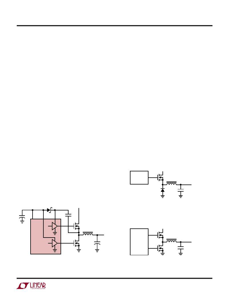
�Synchronous� Operation�
�The� LTC1649� uses� a� synchronous� switching� architecture,�
�with� MOSFET� Q2� taking� the� place� of� the� diode� in� a� classic�
�buck� circuit� (Figure� 3).� This� improves� efficiency� by� reduc-�
�ing� the� voltage� drop� and� the� resultant� power� dissipation�
�across� Q2� to� V� ON� =� (I)(R� DS(ON)(Q2)� ),� usually� much� lower�
�than� V� F� of� the� diode� in� the� classical� circuit.� This� more� than�
�offsets� the� additional� gate� drive� required� by� the� second�
�MOSFET,� allowing� the� LTC1649� to� achieve� efficiencies� in�
�the� mid-90%� range� for� a� wide� range� of� load� currents.�
�Another� feature� of� the� synchronous� architecture� is� that�
�unlike� a� diode,� Q2� can� conduct� current� in� either� direction.�
�This� allows� the� output� of� a� typical� LTC1649� circuit� to� sink�
�current� as� well� as� sourcing� it� while� remaining� in� regula-�
�tion.� The� ability� to� sink� current� at� the� output� allows� the�
�LTC1649� to� be� used� with� reactive� or� other� nonconventional�
�loads� that� may� supply� current� to� the� regulator� as� well� as�
�drawing� current� from� it.�
�V� IN�
�Q1� will� return� to� ground� during� at� least� 7%� of� each� cycle,�
�CONTROLLER�
�Q1�
�ensuring� that� the� charge� pump� will� always� provide� ad-�
�equate� gate� drive� to� Q1.�
�D1�
�V� OUT�
�1649� F03a�
�D� CP�
�V� IN�
�Figure� 3a.� Classical� Buck� Architecture�
�+�
�10� μ� F� CP� OUT�
�PV� CC2�
�PV� CC1�
�G1�
�1� μ� F�
�Q1�
�V� IN�
�L1�
�V� OUT�
�Q1�
�G2�
�Q2�
�+�
�C� OUT�
�CONTROLLER�
�V� OUT�
�Q2�
�LTC1649�
�Figure� 2.� PV� CC1� Charge� Pump�
�1649� F02�
�1649� F03b�
�Figure� 3b.� Synchronous� Buck� Architecture�
�7�
�相关PDF资料 |
PDF描述 |
|---|---|
| MAX810SQ293D3T1G | IC MPU RESET MON 2.93V SOT-323 |
| LTC3853IUJ#PBF | IC REG CTRLR BUCK PWM CM 40-QFN |
| LTC1436AIGN#TRPBF | IC REG CTRLR BUCK PWM CM 24-SSOP |
| LTC1436AIGN#TR | IC REG CTRLR BUCK PWM CM 24-SSOP |
| MAX810SQ293D2T1G | IC MPU RESET MON 2.93V SOT-323 |
相关代理商/技术参数 |
参数描述 |
|---|---|
| LTC1649CS#PBF | 功能描述:IC REG CTRLR BUCK PWM VM 16-SOIC RoHS:是 类别:集成电路 (IC) >> PMIC - 稳压器 - DC DC 切换控制器 系列:- 特色产品:LM3753/54 Scalable 2-Phase Synchronous Buck Controllers 标准包装:1 系列:PowerWise® PWM 型:电压模式 输出数:1 频率 - 最大:1MHz 占空比:81% 电源电压:4.5 V ~ 18 V 降压:是 升压:无 回扫:无 反相:无 倍增器:无 除法器:无 Cuk:无 隔离:无 工作温度:-5°C ~ 125°C 封装/外壳:32-WFQFN 裸露焊盘 包装:Digi-Reel® 产品目录页面:1303 (CN2011-ZH PDF) 其它名称:LM3754SQDKR |
| LTC1649CS#TR | 功能描述:IC REG CTRLR BUCK PWM VM 16-SOIC RoHS:否 类别:集成电路 (IC) >> PMIC - 稳压器 - DC DC 切换控制器 系列:- 标准包装:2,500 系列:- PWM 型:电流模式 输出数:1 频率 - 最大:500kHz 占空比:96% 电源电压:4 V ~ 36 V 降压:无 升压:是 回扫:无 反相:无 倍增器:无 除法器:无 Cuk:无 隔离:无 工作温度:-40°C ~ 125°C 封装/外壳:24-WQFN 裸露焊盘 包装:带卷 (TR) |
| LTC1649CS#TRPBF | 功能描述:IC REG CTRLR BUCK PWM VM 16-SOIC RoHS:否 类别:集成电路 (IC) >> PMIC - 稳压器 - DC DC 切换控制器 系列:- 标准包装:2,500 系列:- PWM 型:电流模式 输出数:1 频率 - 最大:500kHz 占空比:96% 电源电压:4 V ~ 36 V 降压:无 升压:是 回扫:无 反相:无 倍增器:无 除法器:无 Cuk:无 隔离:无 工作温度:-40°C ~ 125°C 封装/外壳:24-WQFN 裸露焊盘 包装:带卷 (TR) |
| LTC1649IS | 功能描述:IC REG CTRLR BUCK PWM VM 16-SOIC RoHS:否 类别:集成电路 (IC) >> PMIC - 稳压器 - DC DC 切换控制器 系列:- 标准包装:4,500 系列:PowerWise® PWM 型:控制器 输出数:1 频率 - 最大:1MHz 占空比:95% 电源电压:2.8 V ~ 5.5 V 降压:是 升压:无 回扫:无 反相:无 倍增器:无 除法器:无 Cuk:无 隔离:无 工作温度:-40°C ~ 125°C 封装/外壳:6-WDFN 裸露焊盘 包装:带卷 (TR) 配用:LM1771EVAL-ND - BOARD EVALUATION LM1771 其它名称:LM1771SSDX |
| LTC1649IS#PBF | 功能描述:IC REG CTRLR BUCK PWM VM 16-SOIC RoHS:是 类别:集成电路 (IC) >> PMIC - 稳压器 - DC DC 切换控制器 系列:- 标准包装:4,500 系列:PowerWise® PWM 型:控制器 输出数:1 频率 - 最大:1MHz 占空比:95% 电源电压:2.8 V ~ 5.5 V 降压:是 升压:无 回扫:无 反相:无 倍增器:无 除法器:无 Cuk:无 隔离:无 工作温度:-40°C ~ 125°C 封装/外壳:6-WDFN 裸露焊盘 包装:带卷 (TR) 配用:LM1771EVAL-ND - BOARD EVALUATION LM1771 其它名称:LM1771SSDX |
发布紧急采购,3分钟左右您将得到回复。