参数资料
| 型号: | LTC1660IN |
| 厂商: | Linear Technology |
| 文件页数: | 18/18页 |
| 文件大小: | 0K |
| 描述: | IC D/A CONV 10BIT OCTAL 16-DIP |
| 标准包装: | 25 |
| 设置时间: | 30µs |
| 位数: | 10 |
| 数据接口: | 串行 |
| 转换器数目: | 8 |
| 电压电源: | 单电源 |
| 功率耗散(最大): | 1mW |
| 工作温度: | -40°C ~ 85°C |
| 安装类型: | 通孔 |
| 封装/外壳: | 16-DIP(0.300",7.62mm) |
| 供应商设备封装: | 16-PDIP |
| 包装: | 管件 |
| 输出数目和类型: | 8 电压,单极;8 电压,双极 |
| 采样率(每秒): | * |
| 产品目录页面: | 1350 (CN2011-ZH PDF) |
LTC1665/LTC1660
9
166560fa
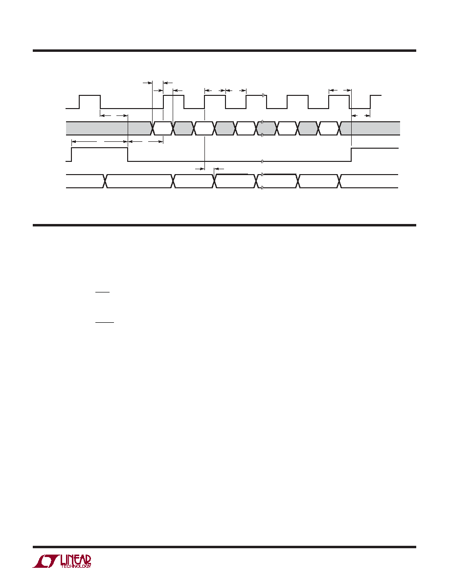
TIMING DIAGRAM
DIN
DOUT
CS/LD
SCK
A3
A2
X1
A1
X0
166560 F01
A1
X1
X0
t2
t8
t9
t11
t5
t7
t6
t1
t3
t4
Figure 1
OPERATION
Transfer Function
The transfer function is:
VOUT(IDEAL) =
k
256
VREF for the LTC1665
VOUT(IDEAL) =
k
1024
VREF for the LTC1660
where k is the decimal equivalent of the binary DAC input
code and VREF is the voltage at REF (Pin 6).
Power-On Reset
The LTC1665 clears the outputs to zero scale when power
is first applied, making system initialization consistent
and repeatable.
Power Supply Sequencing
The voltage at REF (Pin 6) should be kept within the range
– 0.2V ≤ VREF ≤ VCC + 0.2V (see Absolute Maximum Rat-
ings). Particular care should be taken to observe these
limits during power supply turn-on and turn-off sequences,
when the voltage at VCC (Pin 16) is in transition.
Serial Interface
Referring to Figure 2a (2b): With CS/LD held low, data
on the DIN input is shifted into the 16-bit shift register on
the positive edge of SCK. The 4-bit DAC address, A3-A0,
is loaded first (see Table 2), then the 8-bit (10-bit) input
code, D7-D0 (D9-D0), ordered MSB-to-LSB in each case.
Four (two) don’t-care bits, X3-X0 (X1-X0), are loaded last.
When the full 16-bit input word has been shifted in, CS/LD
is pulled high, loading the DAC register with the word
and causing the addressed DAC output(s) to update. The
clock is disabled internally when CS/LD is high. Note: SCK
must be low before CS/LD is pulled low.
The buffered serial output of the shift register is available
on the DOUT pin, which swings from GND to VCC. Data
appears on DOUT 16 positive SCK edges after being ap-
plied to DIN.
Multiple LTC1665/LTC1660’s can be controlled from a
single 3-wire serial port (i.e., SCK, DIN and CS/LD) by
using the included “daisy-chain” facility. A series of m
chips is configured by connecting each DOUT (except the
last) to DIN of the next chip, forming a single 16m-bit
shift register. The SCK and CS/LD signals are common
to all chips in the chain. In use, CS/LD is held low while m
16-bit words are clocked to DIN of the first chip; CS/LD
is then pulled high, updating all of them simultaneously.
相关PDF资料 |
PDF描述 |
|---|---|
| LTC1661IMS8#TRPBF | IC D/A CONV 10BIT MICRPWR 8-MSOP |
| LTC1662IN8#PBF | IC D/A CONV 10BIT MICRPWR 8-DIP |
| LTC1663-1CS5#TRM | IC DAC 10BIT R-R TSOT23-5 |
| LTC1664IN | IC DAC 10BIT QUAD MICRPWR 16DIP |
| LTC1667CG#PBF | IC D/A CONV 14BIT 50MSPS 28-SSOP |
相关代理商/技术参数 |
参数描述 |
|---|---|
| LTC1660IN#PBF | 功能描述:IC D/A CONV 10BIT OCTAL 16-DIP RoHS:是 类别:集成电路 (IC) >> 数据采集 - 数模转换器 系列:- 标准包装:47 系列:- 设置时间:2µs 位数:14 数据接口:并联 转换器数目:1 电压电源:单电源 功率耗散(最大):55µW 工作温度:-40°C ~ 85°C 安装类型:表面贴装 封装/外壳:28-SSOP(0.209",5.30mm 宽) 供应商设备封装:28-SSOP 包装:管件 输出数目和类型:1 电流,单极;1 电流,双极 采样率(每秒):* |
| LTC1661CMS8 | 功能描述:IC D/A CONV 10BIT MICRPWR 8-MSOP RoHS:否 类别:集成电路 (IC) >> 数据采集 - 数模转换器 系列:- 产品培训模块:Data Converter Fundamentals DAC Architectures 设计资源:Unipolar, Precision DC Digital-to-Analog Conversion using AD5450/1/2/3 8-14-Bit DACs (CN0052) Precision, Bipolar, Configuration for AD5450/1/2/3 8-14bit Multiplying DACs (CN0053) AC Signal Processing Using AD5450/1/2/3 Current Output DACs (CN0054) Programmable Gain Element Using AD5450/1/2/3 Current Output DAC Family (CN0055) Single Supply Low Noise LED Current Source Driver Using a Current Output DAC in the Reverse Mode (CN0139) 标准包装:10,000 系列:- 设置时间:- 位数:12 数据接口:DSP,MICROWIRE?,QSPI?,串行,SPI? 转换器数目:1 电压电源:单电源 功率耗散(最大):- 工作温度:-40°C ~ 125°C 安装类型:表面贴装 封装/外壳:SOT-23-8 薄型,TSOT-23-8 供应商设备封装:TSOT-23-8 包装:带卷 (TR) 输出数目和类型:1 电流,单极;1 电流,双极 采样率(每秒):2.7M |
| LTC1661CMS8#PBF | 功能描述:IC D/A CONV 10BIT MICRPWR 8-MSOP RoHS:是 类别:集成电路 (IC) >> 数据采集 - 数模转换器 系列:- 产品培训模块:Data Converter Fundamentals DAC Architectures 标准包装:3,000 系列:nanoDAC™ 设置时间:80µs 位数:18 数据接口:DSP,MICROWIRE?,QSPI?,串行,SPI? 转换器数目:1 电压电源:单电源 功率耗散(最大):- 工作温度:-40°C ~ 105°C 安装类型:表面贴装 封装/外壳:SOT-23-8 供应商设备封装:SOT-23-8 包装:带卷 (TR) 输出数目和类型:1 电压,单极 采样率(每秒):- 产品目录页面:784 (CN2011-ZH PDF) 配用:EVAL-AD5680EBZ-ND - BOARD EVAL FOR AD5680 其它名称:AD5680BRJZ-2REEL7TR |
| LTC1661CMS8#TR | 功能描述:IC DAC 10BIT DUAL MICROPWR 8MSOP RoHS:否 类别:集成电路 (IC) >> 数据采集 - 数模转换器 系列:- 产品培训模块:Data Converter Fundamentals DAC Architectures 设计资源:Unipolar, Precision DC Digital-to-Analog Conversion using AD5450/1/2/3 8-14-Bit DACs (CN0052) Precision, Bipolar, Configuration for AD5450/1/2/3 8-14bit Multiplying DACs (CN0053) AC Signal Processing Using AD5450/1/2/3 Current Output DACs (CN0054) Programmable Gain Element Using AD5450/1/2/3 Current Output DAC Family (CN0055) Single Supply Low Noise LED Current Source Driver Using a Current Output DAC in the Reverse Mode (CN0139) 标准包装:10,000 系列:- 设置时间:- 位数:12 数据接口:DSP,MICROWIRE?,QSPI?,串行,SPI? 转换器数目:1 电压电源:单电源 功率耗散(最大):- 工作温度:-40°C ~ 125°C 安装类型:表面贴装 封装/外壳:SOT-23-8 薄型,TSOT-23-8 供应商设备封装:TSOT-23-8 包装:带卷 (TR) 输出数目和类型:1 电流,单极;1 电流,双极 采样率(每秒):2.7M |
| LTC1661CMS8#TRPBF | 功能描述:IC D/A CONV 10BIT MICRPWR 8-MSOP RoHS:是 类别:集成电路 (IC) >> 数据采集 - 数模转换器 系列:- 产品培训模块:Data Converter Fundamentals DAC Architectures 设计资源:Unipolar, Precision DC Digital-to-Analog Conversion using AD5450/1/2/3 8-14-Bit DACs (CN0052) Precision, Bipolar, Configuration for AD5450/1/2/3 8-14bit Multiplying DACs (CN0053) AC Signal Processing Using AD5450/1/2/3 Current Output DACs (CN0054) Programmable Gain Element Using AD5450/1/2/3 Current Output DAC Family (CN0055) Single Supply Low Noise LED Current Source Driver Using a Current Output DAC in the Reverse Mode (CN0139) 标准包装:10,000 系列:- 设置时间:- 位数:12 数据接口:DSP,MICROWIRE?,QSPI?,串行,SPI? 转换器数目:1 电压电源:单电源 功率耗散(最大):- 工作温度:-40°C ~ 125°C 安装类型:表面贴装 封装/外壳:SOT-23-8 薄型,TSOT-23-8 供应商设备封装:TSOT-23-8 包装:带卷 (TR) 输出数目和类型:1 电流,单极;1 电流,双极 采样率(每秒):2.7M |
发布紧急采购,3分钟左右您将得到回复。