- 您现在的位置:买卖IC网 > PDF目录15260 > LTC1698EGN#TR (Linear Technology)IC REG CTRLR ISO PWM CM 16-SSOP PDF资料下载
参数资料
| 型号: | LTC1698EGN#TR |
| 厂商: | Linear Technology |
| 文件页数: | 11/24页 |
| 文件大小: | 0K |
| 描述: | IC REG CTRLR ISO PWM CM 16-SSOP |
| 标准包装: | 2,500 |
| PWM 型: | 电流模式 |
| 输出数: | 1 |
| 频率 - 最大: | 400kHz |
| 电源电压: | 6 V ~ 12.6 V |
| 降压: | 是 |
| 升压: | 无 |
| 回扫: | 无 |
| 反相: | 无 |
| 倍增器: | 无 |
| 除法器: | 无 |
| Cuk: | 无 |
| 隔离: | 是 |
| 工作温度: | -40°C ~ 85°C |
| 封装/外壳: | 16-SSOP(0.154",3.90mm 宽) |
| 包装: | 带卷 (TR) |
| 其它名称: | LTC1698EGNTR |
�� �
�
�LTC1698�
�APPLICATIO� S� I� FOR� ATIO�
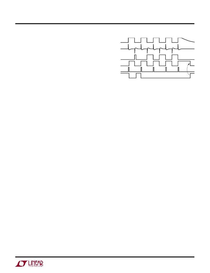
�drivers� TG� and� BG� go� high.� The� pulse� transformer� T2�
�generates� a� negative� slew� at� the� SYNC� pin� and� forces� the�
�secondary� MOSFET� driver� FG� to� go� high� and� CG� to� go� low.�
�When� TG� and� BG� go� low,� SG� goes� high� and� the� secondary�
�controller� forces� CG� high� and� FG� low.�
�For� a� given� pulse� transformer,� a� bigger� capacitor� C� SG�
�generates� a� higher� and� wider� SYNC� pulse.� The� peak� of� this�
�SG�
�SYNC�
�FG�
�CG�
�RESET�
�(INTERNAL)�
�pulse� should� be� much� higher� than� the� SYNC� threshold.�
�Amplitudes� greater� than� ±� 5V� help� to� speed� up� the� SYNC�
�DISDRI�
�(INTERNAL)�
�1698� F05�
�comparator� and� reduce� the� SYNC� to� FG� and� CG� drivers�
�propagation� delay.� The� minimum� pulse� width� is� 75ns.�
�Overshoot� during� the� pulse� transformer� reset� interval�
�must� be� minimized� and� kept� below� the� minimum� com-�
�parator� thresholds� of� ±� 1V.� The� amount� of� overshoot� can�
�be� reduced� by� having� a� smaller� reset� resistor� R� SYNC� .� For�
�nonisolated� applications,� the� SYNC� input� can� be� driven�
�directly� by� a� square� pulse.� To� reduce� the� propagation�
�delay,� make� the� positive� and� negative� magnitude� of� the�
�square� wave� much� greater� than� the� ±� 2.2V� maximum�
�threshold.�
�In� addition� to� the� simple� driver� synchronization,� the� sec-�
�ondary� controller� requires� a� driver� disable� signal.� Loss� of�
�synchronization� while� CG� is� high� will� cause� Q4� to� dis-�
�charge� the� output� capacitor.� This� produces� a� negative�
�output� voltage� transient� and� possible� damage� to� the� load�
�circuitry� connected� to� V� OUT� .� To� overcome� this� problem,�
�the� LTC1698� comes� with� a� unique� adaptive� time-out�
�circuit.� It� works� well� within� the� 50kHz� to� 400kHz� frequency�
�range.� At� every� positive� SYNC� pulse,� the� internal� timer�
�resets.� If� the� SYNC� signal� is� missing,� the� internal� timer�
�loses� its� reset� command,� and� eventually� exceeds� the�
�internal� time-out� limit.� This� forces� both� the� FG� and� CG�
�drivers� to� go� low� immediately.�
�The� time-out� duration� varies� linearly� with� the� LT3781�
�primary� controller� clocking� frequency.� Upon� power� up,�
�the� time-out� circuitry� takes� a� few� clock� cycles� to� adapt� to�
�the� input� clock� frequency.� During� this� time� interval,� the�
�drivers� pulse� width� might� be� prematurely� terminated,� and�
�the� inductor� current� flows� through� the� MOSFETs� body�
�diode.� Once� the� LTC1698� timer� locks� to� the� clocking�
�frequency,� the� LTC1698� drivers� follow� the� SYNC� signal�
�without� fail.� Figure� 5� shows� the� SYNC� time-out� wave-�
�Figure� 5.� SYNC� Time-Out� Waveforms�
�forms.� The� time-out� circuit� guarantees� that� if� the� SYNC�
�pulse� is� missing� for� more� than� one� period,� both� the�
�drivers� will� be� shut� down� preventing� the� output� voltage�
�from� going� below� ground.� The� wide� synchronization�
�frequency� range� adds� flexibility� to� the� forward� converter�
�and� allows� this� converter� chip� set� to� meet� different�
�application� requirements.�
�Under� normal� operating� conditions,� the� time-out� circuitry�
�adapts� to� the� switching� frequency� within� a� few� cycles.�
�Once� synchronized,� internal� circuitry� ensures� the� maxi-�
�mum� time� that� the� Catch� FET� (Q4)� could� be� left� turned� on�
�is� typically� just� over� one� switching� period.� This� is� particu-�
�larly� important� with� high� output� voltages� that� can� generate�
�significant� negative� output� inductor� currents� if� the� Catch�
�FET� Q4� is� left� on.� Poor� feedback� loop� performance� includ-�
�ing� output� voltage� overshoot� can� cause� the� primary� con-�
�troller� to� interrupt� the� synchronization� pulse� train.� While�
�this� generally� is� not� a� problem,� it� is� possible� that� low�
�frequency� interruptions� could� lead� to� a� time-out� period�
�longer� than� a� switching� period,� limited� only� by� the� internal�
�timer� clamp� (50� μ� s� typical).�
�Output� Voltage� Programming�
�The� switching� regulator� output� voltage� is� programmed�
�through� a� resistor� feedback� network� (R1� and� R2� in�
�Figure� 1)� connected� to� V� FB� .� If� the� output� is� at� its� nominal�
�value,� the� divider� output� is� regulated� to� the� error� amplifier�
�threshold� of� 1.233V.�
�The� output� voltage� is� thus� set� according� to� the� relation:�
�V� OUT� =� 1.233� ?� (1� +� R2/R1)�
�1698f�
�11�
�相关PDF资料 |
PDF描述 |
|---|---|
| EYM06DRMD-S273 | CONN EDGECARD 12POS .156 WW |
| LTC1922EG-1#TRPBF | IC REG CTRLR ISO PWM 20-SSOP |
| LTC1698EGN#TRPBF | IC REG CTRLR ISO PWM CM 16-SSOP |
| NCP301LSN46T1G | IC VOLT DETECT OD 4.6V 5TSOP |
| LTC3722EGN-2#TR | IC REG CTRLR DIV ISO PWM 24SSOP |
相关代理商/技术参数 |
参数描述 |
|---|---|
| LTC1698ES | 功能描述:IC REG CTRLR ISO PWM CM 16-SOIC RoHS:否 类别:集成电路 (IC) >> PMIC - 稳压器 - DC DC 切换控制器 系列:- 标准包装:2,000 系列:- PWM 型:电流模式 输出数:1 频率 - 最大:1MHz 占空比:50% 电源电压:9 V ~ 10 V 降压:无 升压:是 回扫:是 反相:无 倍增器:无 除法器:无 Cuk:无 隔离:无 工作温度:-40°C ~ 85°C 封装/外壳:8-TSSOP(0.173",4.40mm 宽) 包装:带卷 (TR) |
| LTC1698ES#PBF | 功能描述:IC REG CTRLR ISO PWM CM 16-SOIC RoHS:是 类别:集成电路 (IC) >> PMIC - 稳压器 - DC DC 切换控制器 系列:- 标准包装:2,000 系列:- PWM 型:电流模式 输出数:1 频率 - 最大:1MHz 占空比:50% 电源电压:9 V ~ 10 V 降压:无 升压:是 回扫:是 反相:无 倍增器:无 除法器:无 Cuk:无 隔离:无 工作温度:-40°C ~ 85°C 封装/外壳:8-TSSOP(0.173",4.40mm 宽) 包装:带卷 (TR) |
| LTC1698ES#TR | 功能描述:IC REG CTRLR ISO PWM CM 16-SOIC RoHS:否 类别:集成电路 (IC) >> PMIC - 稳压器 - DC DC 切换控制器 系列:- 标准包装:4,500 系列:PowerWise® PWM 型:控制器 输出数:1 频率 - 最大:1MHz 占空比:95% 电源电压:2.8 V ~ 5.5 V 降压:是 升压:无 回扫:无 反相:无 倍增器:无 除法器:无 Cuk:无 隔离:无 工作温度:-40°C ~ 125°C 封装/外壳:6-WDFN 裸露焊盘 包装:带卷 (TR) 配用:LM1771EVAL-ND - BOARD EVALUATION LM1771 其它名称:LM1771SSDX |
| LTC1698ES#TRPBF | 功能描述:IC REG CTRLR ISO PWM CM 16-SOIC RoHS:是 类别:集成电路 (IC) >> PMIC - 稳压器 - DC DC 切换控制器 系列:- 标准包装:4,500 系列:PowerWise® PWM 型:控制器 输出数:1 频率 - 最大:1MHz 占空比:95% 电源电压:2.8 V ~ 5.5 V 降压:是 升压:无 回扫:无 反相:无 倍增器:无 除法器:无 Cuk:无 隔离:无 工作温度:-40°C ~ 125°C 封装/外壳:6-WDFN 裸露焊盘 包装:带卷 (TR) 配用:LM1771EVAL-ND - BOARD EVALUATION LM1771 其它名称:LM1771SSDX |
| LTC1698IGN | 功能描述:IC REG CTRLR ISO PWM CM 16-SSOP RoHS:否 类别:集成电路 (IC) >> PMIC - 稳压器 - DC DC 切换控制器 系列:- 标准包装:4,500 系列:PowerWise® PWM 型:控制器 输出数:1 频率 - 最大:1MHz 占空比:95% 电源电压:2.8 V ~ 5.5 V 降压:是 升压:无 回扫:无 反相:无 倍增器:无 除法器:无 Cuk:无 隔离:无 工作温度:-40°C ~ 125°C 封装/外壳:6-WDFN 裸露焊盘 包装:带卷 (TR) 配用:LM1771EVAL-ND - BOARD EVALUATION LM1771 其它名称:LM1771SSDX |
发布紧急采购,3分钟左右您将得到回复。