- 您现在的位置:买卖IC网 > PDF目录15260 > LTC1698EGN#TR (Linear Technology)IC REG CTRLR ISO PWM CM 16-SSOP PDF资料下载
参数资料
| 型号: | LTC1698EGN#TR |
| 厂商: | Linear Technology |
| 文件页数: | 12/24页 |
| 文件大小: | 0K |
| 描述: | IC REG CTRLR ISO PWM CM 16-SSOP |
| 标准包装: | 2,500 |
| PWM 型: | 电流模式 |
| 输出数: | 1 |
| 频率 - 最大: | 400kHz |
| 电源电压: | 6 V ~ 12.6 V |
| 降压: | 是 |
| 升压: | 无 |
| 回扫: | 无 |
| 反相: | 无 |
| 倍增器: | 无 |
| 除法器: | 无 |
| Cuk: | 无 |
| 隔离: | 是 |
| 工作温度: | -40°C ~ 85°C |
| 封装/外壳: | 16-SSOP(0.154",3.90mm 宽) |
| 包装: | 带卷 (TR) |
| 其它名称: | LTC1698EGNTR |
�� �
�
�LTC1698�
�APPLICATIO� S� I� FOR� ATIO�
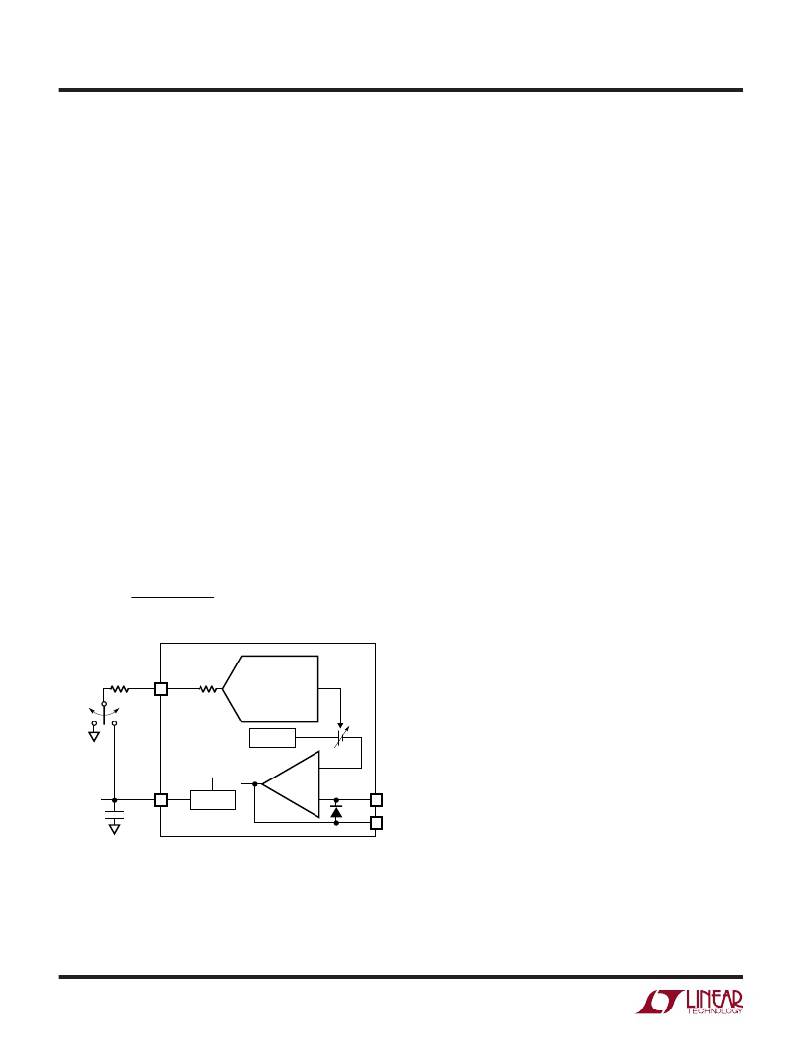
�MARGIN� Adjustment�
�The� MARGIN� input� is� used� for� adjusting� the� programmed�
�output� voltage� linearly� by� varying� the� current� flowing� into�
�and� out� of� the� pin.� Forcing� 100� μ� A� into� the� pin� moves� the�
�output� voltage� 5%� higher.� Forcing� 100� μ� A� out� of� the� pin�
�moves� the� output� voltage� 5%� lower.� With� the� MARGIN� pin�
�floating,� the� V� FB� pin� is� regulated� to� the� bandgap� voltage� of�
�1.233V.� The� MARGIN� pin� is� a� high� impedance� input.� It� is�
�important� to� keep� this� pin� away� from� any� noise� source� like�
�the� inductor� switching� node.� Any� stray� signal� coupled� to�
�the� MARGIN� pin� can� affect� the� switching� regulator� output�
�voltage.�
�This� pin� is� internally� connected� to� a� 16.5k� resistor� that�
�feeds� the� I-V� converter.� The� I-V� converter� output� linearly�
�controls� the� error� amplifier� offset� voltage.� The� input� of� the�
�I-V� converter� is� biased� at� 1.65V.� This� allows� the� ±� 100� μ� A�
�current� to� be� obtained� by� connecting� the� MARGIN� pin� to�
�the� V� AUX� 3.3V� supply� (+� 5%)� or� GND� (–� 5%).� For� output�
�voltage� adjustment� smaller� than� ±� 5%,� an� external� resistor�
�R� EXT� as� shown� in� Figure� 6� is� added� in� series� with� the�
�internal� resistor� to� lower� the� current� flowing� into� or� out� of�
�the� MARGIN� pin.� The� value� of� R� EXT� is� calculated� as� follow:�
�V� FB� loop� causes� the� error� amplifier� to� drive� the� OPTODRV�
�pin� low,� forcing� the� primary� controller� to� increase� the� duty�
�cycle.� This� causes� the� output� voltage� to� increase� to� a�
�dangerously� high� level.� To� eliminate� this� fault� condition,�
�the� OVP� comparator� monitors� the� output� voltage� with� a�
�resistive� divider� at� OVPIN.� A� voltage� at� OVPIN� higher� than�
�the� V� REF� potential� forces� the� OPTODRV� pin� high� and�
�reduces� the� duty� cycle,� thus� preventing� the� output� voltage�
�from� increasing� further.�
�The� OVPIN� senses� the� output� voltage� through� a� resistor�
�divider� network� (R4� and� R5� in� Figure� 1).� The� divider� is�
�ratioed� such� that� the� voltage� at� OVPIN� equals� 1.233V� when�
�the� output� voltage� rises� to� the� overvoltage� level.� The�
�overvoltage� level� is� set� following� the� relation:�
�V� OVERVOLTAGE� =� 1.233� ?� (1� +� R5/R4)�
�The� OVP� comparator� is� designed� to� respond� quickly� to� an�
�overvoltage� condition.� A� small� capacitor� from� OVPIN� to�
�ground� keeps� any� noise� spikes� from� coupling� to� the� OVP�
�pin.� This� simple� RC� filter� prevents� a� momentary� overshoot�
�from� triggering� the� OVP� comparator.�
�The� OVP� comparator� threshold� is� independent� of� the�
�potential� at� the� MARGIN� pin.� If� the� OVP� function� is� not�
�R� EXT� =� ?�
�–� 1� ?� ?� 16� .� 5� k�
�?� 5� %�
�?� REQUIRED� %�
�?�
�?�
�used,� connect� OVPIN� to� ground.�
�Power� Good�
�The� PWRGD� pin� is� an� open-drain� output� for� power� good�
�REDUCE�
�V� FB�
�R� EXT�
�(OPTIONAL)�
�INCREASE�
�V� FB�
�7�
�R� MARGIN�
�MARGIN�
�I-V� CONVERTER�
�BANDGAP�
�V� REF�
�indication.� PWRGD� floats� if� V� FB� is� above� 94%� of� the�
�nominal� value� for� more� than� 2ms.� An� external� pull-up�
�resistor� is� required� for� PWRGD� to� swing� high.� PWRGD�
�pulls� low� if� V� FB� drops� below� 94%� of� the� nominal� value� for�
�more� than� 1ms.� The� PWRGD� threshold� is� referenced� to� the�
�±� 5%� V� REF�
�1.233V� bandgap� voltage,� which� remains� unchanged� if� the�
�V� DD�
�ERR�
�+�
�MARGIN� pin� is� exercised.�
�V� AUX�
�3.3V�
�14� AUX� GEN� –�
�V� AUX�
�0.1� μ� F�
�Figure� 6.� Output� Voltage� Adjustment�
�V� FB�
�8�
�V� COMP�
�6�
�1698� F06�
�Opto� Feedback� and� Frequency� Compensation�
�For� a� forward� converter� to� obtain� good� load� and� line�
�regulation,� the� output� voltage� must� be� sensed� and� com-�
�pared� to� an� accurate� reference� potential.� Any� error� voltage�
�Overvoltage� Function�
�The� OVPIN� is� used� for� overvoltage� protection� and� is�
�designed� to� protect� against� an� open� V� FB� loop.� Opening� the�
�must� be� amplified� and� fed� back� to� the� supply’s� control�
�circuitry� where� the� sensed� error� can� be� corrected.� In� an�
�isolated� supply,� the� control� circuitry� is� frequently� located�
�on� the� primary.� The� output� error� signal� in� this� type� of�
�1698f�
�12�
�相关PDF资料 |
PDF描述 |
|---|---|
| EYM06DRMD-S273 | CONN EDGECARD 12POS .156 WW |
| LTC1922EG-1#TRPBF | IC REG CTRLR ISO PWM 20-SSOP |
| LTC1698EGN#TRPBF | IC REG CTRLR ISO PWM CM 16-SSOP |
| NCP301LSN46T1G | IC VOLT DETECT OD 4.6V 5TSOP |
| LTC3722EGN-2#TR | IC REG CTRLR DIV ISO PWM 24SSOP |
相关代理商/技术参数 |
参数描述 |
|---|---|
| LTC1698ES | 功能描述:IC REG CTRLR ISO PWM CM 16-SOIC RoHS:否 类别:集成电路 (IC) >> PMIC - 稳压器 - DC DC 切换控制器 系列:- 标准包装:2,000 系列:- PWM 型:电流模式 输出数:1 频率 - 最大:1MHz 占空比:50% 电源电压:9 V ~ 10 V 降压:无 升压:是 回扫:是 反相:无 倍增器:无 除法器:无 Cuk:无 隔离:无 工作温度:-40°C ~ 85°C 封装/外壳:8-TSSOP(0.173",4.40mm 宽) 包装:带卷 (TR) |
| LTC1698ES#PBF | 功能描述:IC REG CTRLR ISO PWM CM 16-SOIC RoHS:是 类别:集成电路 (IC) >> PMIC - 稳压器 - DC DC 切换控制器 系列:- 标准包装:2,000 系列:- PWM 型:电流模式 输出数:1 频率 - 最大:1MHz 占空比:50% 电源电压:9 V ~ 10 V 降压:无 升压:是 回扫:是 反相:无 倍增器:无 除法器:无 Cuk:无 隔离:无 工作温度:-40°C ~ 85°C 封装/外壳:8-TSSOP(0.173",4.40mm 宽) 包装:带卷 (TR) |
| LTC1698ES#TR | 功能描述:IC REG CTRLR ISO PWM CM 16-SOIC RoHS:否 类别:集成电路 (IC) >> PMIC - 稳压器 - DC DC 切换控制器 系列:- 标准包装:4,500 系列:PowerWise® PWM 型:控制器 输出数:1 频率 - 最大:1MHz 占空比:95% 电源电压:2.8 V ~ 5.5 V 降压:是 升压:无 回扫:无 反相:无 倍增器:无 除法器:无 Cuk:无 隔离:无 工作温度:-40°C ~ 125°C 封装/外壳:6-WDFN 裸露焊盘 包装:带卷 (TR) 配用:LM1771EVAL-ND - BOARD EVALUATION LM1771 其它名称:LM1771SSDX |
| LTC1698ES#TRPBF | 功能描述:IC REG CTRLR ISO PWM CM 16-SOIC RoHS:是 类别:集成电路 (IC) >> PMIC - 稳压器 - DC DC 切换控制器 系列:- 标准包装:4,500 系列:PowerWise® PWM 型:控制器 输出数:1 频率 - 最大:1MHz 占空比:95% 电源电压:2.8 V ~ 5.5 V 降压:是 升压:无 回扫:无 反相:无 倍增器:无 除法器:无 Cuk:无 隔离:无 工作温度:-40°C ~ 125°C 封装/外壳:6-WDFN 裸露焊盘 包装:带卷 (TR) 配用:LM1771EVAL-ND - BOARD EVALUATION LM1771 其它名称:LM1771SSDX |
| LTC1698IGN | 功能描述:IC REG CTRLR ISO PWM CM 16-SSOP RoHS:否 类别:集成电路 (IC) >> PMIC - 稳压器 - DC DC 切换控制器 系列:- 标准包装:4,500 系列:PowerWise® PWM 型:控制器 输出数:1 频率 - 最大:1MHz 占空比:95% 电源电压:2.8 V ~ 5.5 V 降压:是 升压:无 回扫:无 反相:无 倍增器:无 除法器:无 Cuk:无 隔离:无 工作温度:-40°C ~ 125°C 封装/外壳:6-WDFN 裸露焊盘 包装:带卷 (TR) 配用:LM1771EVAL-ND - BOARD EVALUATION LM1771 其它名称:LM1771SSDX |
发布紧急采购,3分钟左右您将得到回复。