- 您现在的位置:买卖IC网 > PDF目录14142 > LTC1701ES5#TR (Linear Technology)IC REG BUCK ADJ 0.5A TSOT23-5 PDF资料下载
参数资料
| 型号: | LTC1701ES5#TR |
| 厂商: | Linear Technology |
| 文件页数: | 8/12页 |
| 文件大小: | 0K |
| 描述: | IC REG BUCK ADJ 0.5A TSOT23-5 |
| 标准包装: | 2,500 |
| 类型: | 降压(降压) |
| 输出类型: | 可调式 |
| 输出数: | 1 |
| 输出电压: | 1.25 V ~ 5 V |
| 输入电压: | 2.5 V ~ 5.5 V |
| PWM 型: | 电流模式,混合 |
| 频率 - 开关: | 1MHz |
| 电流 - 输出: | 500mA |
| 同步整流器: | 无 |
| 工作温度: | -40°C ~ 85°C |
| 安装类型: | 表面贴装 |
| 封装/外壳: | SOT-23-5 细型,TSOT-23-5 |
| 包装: | 带卷 (TR) |
| 供应商设备封装: | TSOT-23-5 |
�� �
�
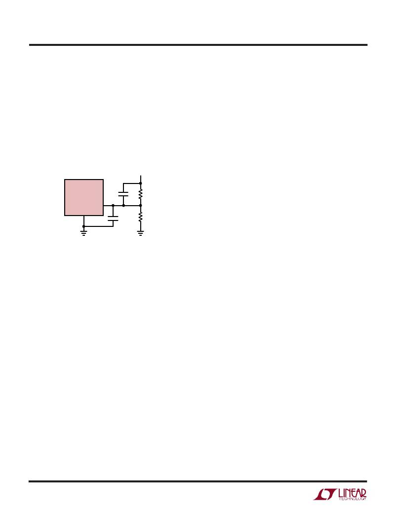
�LTC1701/LTC1701B�
�APPLICATIO� S� I� FOR� ATIO�
�Figure� 2.� The� output� voltage� is� set� by� a� resistive� divider�
�according� to� the� following� formula:�
�V� OUT� =� 1.25V(1� +� R2/R1)�
�To� prevent� stray� pickup,� a� capacitor� of� about� 5pF� can� be�
�added� across� R1,� located� close� to� the� LTC1701.� Unfortu-�
�nately,� the� load� step� response� is� degraded� by� this� capaci-�
�tor.� Using� a� good� printed� circuit� board� layout� eliminates�
�the� need� for� this� capacitor.� Great� care� should� be� taken� to�
�route� the� V� FB� line� away� from� noise� sources,� such� as� the�
�inductor� or� the� SW� line.�
�V� OUT�
�of� 20%� to� 100%� of� full-load� current� having� a� rise� time� of�
�1� μ� s� to� 10� μ� s� will� produce� output� voltage� and� I� TH� pin�
�waveforms� that� will� give� a� sense� of� the� overall� loop�
�stability� without� breaking� the� feedback� loop.�
�The� initial� output� voltage� step� may� not� be� within� the�
�bandwidth� of� the� feedback� loop,� so� the� standard� second-�
�order� overshoot/DC� ratio� cannot� be� used� to� determine�
�phase� margin.� The� gain� of� the� loop� increases� with� R3� and�
�the� bandwidth� of� the� loop� increases� with� decreasing� C3.� If�
�R3� is� increased� by� the� same� factor� that� C3� is� decreased,�
�the� zero� frequency� will� be� kept� the� same,� thereby� keeping�
�the� phase� the� same� in� the� most� critical� frequency� range� of�
�LTC1701�
�SGND�
�V� FB�
�5pF�
�C� F�
�R2�
�1%�
�R1�
�1%�
�the� feedback� loop.� In� addition,� a� feed-forward� capacitor,�
�C� F� ,� can� be� added� to� improve� the� high� frequency� response,�
�as� shown� in� Figure� 2.� Capacitor� C� F� provides� phase� lead� by�
�creating� a� high� frequency� zero� with� R2� which� improves� the�
�phase� margin.�
�1701� F02�
�Figure� 2.� Setting� the� Output� Voltage�
�Transient� Response�
�The� OPTI-LOOP� compensation� allows� the� transient� re-�
�sponse� to� be� optimized� for� a� wide� range� of� loads� and�
�output� capacitors.� The� availability� of� the� I� TH� pin� not� only�
�allows� optimization� of� the� control� loop� behavior� but� also�
�provides� a� DC� coupled� and� AC� filtered� closed-loop� re-�
�sponse� test� point.� The� DC� step,� rise� time� and� settling� at� this�
�test� point� truly� reflects� the� closed-loop� response.� Assum-�
�ing� a� predominately� second� order� system,� phase� margin�
�and/or� damping� factor� can� be� estimated� using� the� percent-�
�age� of� overshoot� seen� at� this� pin.� The� bandwidth� can� also�
�be� estimated� by� examining� the� rise� time� at� the� pin.�
�The� I� TH� external� components� shown� in� the� Figure� 1� circuit�
�will� provide� an� adequate� starting� point� for� most� applica-�
�tions.� The� series� R3-C3� filter� sets� the� dominant� pole-zero�
�loop� compensation.� The� values� can� be� modified� slightly�
�(from� 0.5� to� 2� times� their� suggested� values)� to� optimize�
�transient� response� once� the� final� PC� layout� is� done� and� the�
�particular� output� capacitor� type� and� value� have� been�
�determined.� The� output� capacitors� need� to� be� selected�
�because� the� various� types� and� values� determine� the� loop�
�feedback� factor� gain� and� phrase.� An� output� current� pulse�
�8�
�The� output� voltage� settling� behavior� is� related� to� the�
�stability� of� the� closed-loop� system� and� will� demonstrate�
�the� actual� overall� supply� performance.� For� a� detailed�
�explanation� of� optimizing� the� compensation� components,�
�including� a� review� of� control� loop� theory,� refer� to� Applica-�
�tion� Note� 76.�
�RUN� Function�
�The� I� TH� /RUN� pin� is� a� dual� purpose� pin� that� provides� the�
�loop� compensation� and� a� means� to� shut� down� the� LTC1701.�
�Soft-start� can� also� be� implemented� with� this� pin.� Soft-start�
�reduces� surge� currents� from� V� IN� by� gradually� increasing�
�the� internal� peak� inductor� current.� Power� supply� sequenc-�
�ing� can� also� be� accomplished� using� this� pin.�
�An� external� pull-up� is� required� to� charge� the� external�
�capacitor� C3� in� Figure� 1.� Typically,� a� 1M� resistor� between�
�V� IN� and� I� TH� /RUN� is� used.� When� the� voltage� on� I� TH� /RUN�
�reaches� about� 0.8V� the� LTC1701� begins� operating.� At� this�
�point� the� error� amplifier� pulls� up� the� I� TH� /RUN� pin� to� the�
�normal� operating� range� of� 1.25V� to� 2.25V.�
�Soft-start� can� be� implemented� by� ramping� the� voltage� on�
�I� TH� /RUN� during� start-up� as� shown� in� Figure� 3(b).� As� the�
�voltage� on� I� TH� /RUN� ramps� through� its� operating� range� the�
�internal� peak� current� limit� is� also� ramped� at� a� proportional�
�linear� rate.�
�相关PDF资料 |
PDF描述 |
|---|---|
| MAX6867UK18D5L+T | IC MPU SUPERVISOR SOT23-5 |
| LNC2H332MSEH | CAP ALUM 3300UF 500V 20% SCREW |
| VE-BNX-EX-F2 | CONVERTER MOD DC/DC 5.2V 75W |
| LNY2G682MSEG | CAP ALUM 6800UF 400V 20% SCREW |
| VE-BNX-EW-F2 | CONVERTER MOD DC/DC 5.2V 100W |
相关代理商/技术参数 |
参数描述 |
|---|---|
| LTC1702ACGN | 功能描述:IC REG CTRLR BUCK PWM VM 24-SSOP RoHS:否 类别:集成电路 (IC) >> PMIC - 稳压器 - DC DC 切换控制器 系列:PolyPhase® 标准包装:4,500 系列:PowerWise® PWM 型:控制器 输出数:1 频率 - 最大:1MHz 占空比:95% 电源电压:2.8 V ~ 5.5 V 降压:是 升压:无 回扫:无 反相:无 倍增器:无 除法器:无 Cuk:无 隔离:无 工作温度:-40°C ~ 125°C 封装/外壳:6-WDFN 裸露焊盘 包装:带卷 (TR) 配用:LM1771EVAL-ND - BOARD EVALUATION LM1771 其它名称:LM1771SSDX |
| LTC1702ACGN#PBF | 功能描述:IC REG CTRLR BUCK PWM VM 24-SSOP RoHS:是 类别:集成电路 (IC) >> PMIC - 稳压器 - DC DC 切换控制器 系列:PolyPhase® 标准包装:4,500 系列:PowerWise® PWM 型:控制器 输出数:1 频率 - 最大:1MHz 占空比:95% 电源电压:2.8 V ~ 5.5 V 降压:是 升压:无 回扫:无 反相:无 倍增器:无 除法器:无 Cuk:无 隔离:无 工作温度:-40°C ~ 125°C 封装/外壳:6-WDFN 裸露焊盘 包装:带卷 (TR) 配用:LM1771EVAL-ND - BOARD EVALUATION LM1771 其它名称:LM1771SSDX |
| LTC1702ACGN#TR | 功能描述:IC REG CTRLR BUCK PWM VM 24-SSOP RoHS:否 类别:集成电路 (IC) >> PMIC - 稳压器 - DC DC 切换控制器 系列:PolyPhase® 标准包装:4,500 系列:PowerWise® PWM 型:控制器 输出数:1 频率 - 最大:1MHz 占空比:95% 电源电压:2.8 V ~ 5.5 V 降压:是 升压:无 回扫:无 反相:无 倍增器:无 除法器:无 Cuk:无 隔离:无 工作温度:-40°C ~ 125°C 封装/外壳:6-WDFN 裸露焊盘 包装:带卷 (TR) 配用:LM1771EVAL-ND - BOARD EVALUATION LM1771 其它名称:LM1771SSDX |
| LTC1702ACGN#TRPBF | 功能描述:IC REG CTRLR BUCK PWM VM 24-SSOP RoHS:是 类别:集成电路 (IC) >> PMIC - 稳压器 - DC DC 切换控制器 系列:PolyPhase® 标准包装:4,500 系列:PowerWise® PWM 型:控制器 输出数:1 频率 - 最大:1MHz 占空比:95% 电源电压:2.8 V ~ 5.5 V 降压:是 升压:无 回扫:无 反相:无 倍增器:无 除法器:无 Cuk:无 隔离:无 工作温度:-40°C ~ 125°C 封装/外壳:6-WDFN 裸露焊盘 包装:带卷 (TR) 配用:LM1771EVAL-ND - BOARD EVALUATION LM1771 其它名称:LM1771SSDX |
| LTC1702AIGN | 功能描述:IC REG CTRLR BUCK PWM VM 24-SSOP RoHS:否 类别:集成电路 (IC) >> PMIC - 稳压器 - DC DC 切换控制器 系列:PolyPhase® 标准包装:4,500 系列:PowerWise® PWM 型:控制器 输出数:1 频率 - 最大:1MHz 占空比:95% 电源电压:2.8 V ~ 5.5 V 降压:是 升压:无 回扫:无 反相:无 倍增器:无 除法器:无 Cuk:无 隔离:无 工作温度:-40°C ~ 125°C 封装/外壳:6-WDFN 裸露焊盘 包装:带卷 (TR) 配用:LM1771EVAL-ND - BOARD EVALUATION LM1771 其它名称:LM1771SSDX |
发布紧急采购,3分钟左右您将得到回复。