- 您现在的位置:买卖IC网 > PDF目录14142 > LTC1701ES5#TR (Linear Technology)IC REG BUCK ADJ 0.5A TSOT23-5 PDF资料下载
参数资料
| 型号: | LTC1701ES5#TR |
| 厂商: | Linear Technology |
| 文件页数: | 9/12页 |
| 文件大小: | 0K |
| 描述: | IC REG BUCK ADJ 0.5A TSOT23-5 |
| 标准包装: | 2,500 |
| 类型: | 降压(降压) |
| 输出类型: | 可调式 |
| 输出数: | 1 |
| 输出电压: | 1.25 V ~ 5 V |
| 输入电压: | 2.5 V ~ 5.5 V |
| PWM 型: | 电流模式,混合 |
| 频率 - 开关: | 1MHz |
| 电流 - 输出: | 500mA |
| 同步整流器: | 无 |
| 工作温度: | -40°C ~ 85°C |
| 安装类型: | 表面贴装 |
| 封装/外壳: | SOT-23-5 细型,TSOT-23-5 |
| 包装: | 带卷 (TR) |
| 供应商设备封装: | TSOT-23-5 |
�� �
�
�LTC1701/LTC1701B�
�APPLICATIO� S� I� FOR� ATIO�
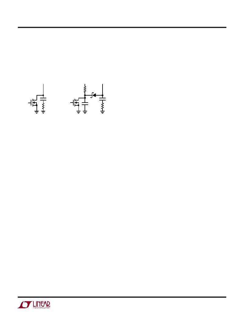
�During� normal� operation� the� voltage� on� the� I� TH� /RUN� pin�
�will� vary� from� 1.25V� to� 2.25V� depending� on� the� load�
�current.� Pulling� the� I� TH� /RUN� pin� below� 0.8V� puts� the�
�LTC1701� into� a� low� quiescent� current� shutdown� mode�
�(I� Q� <� 1� μ� A).� This� pin� can� be� driven� directly� from� logic� as�
�shown� in� Figures� 3(a).�
�continuous� mode,� I� GATECHG� =� f� ?� Q� P� ,� where� Q� P� is� the� gate�
�charge� of� the� internal� MOSFET� switch.�
�3)� I� 2� R� Losses� are� predicted� from� the� DC� resistances� of� the�
�MOSFET� and� inductor.� In� continuous� mode� the� average�
�output� current� flows� through� L,� but� is� “chopped”� between�
�the� topside� internal� MOSFET� and� the� Schottky� diode.� At�
�I� TH� /RUN�
�C� C�
�R1�
�D1�
�I� TH� /RUN�
�C� C�
�low� supply� voltages� where� the� switch� on-resistance� is�
�higher� and� the� switch� is� on� for� longer� periods� due� to� the�
�higher� duty� cycle,� the� switch� losses� will� dominate.� Using�
�a� larger� inductance� helps� minimize� these� switch� losses.� At�
�(a)�
�R� C�
�C1�
�(b)�
�R� C�
�1701� F03�
�high� supply� voltages,� these� losses� are� proportional� to� the�
�load.� I� 2� R� losses� cause� the� efficiency� to� drop� at� high� output�
�currents.�
�Figure� 3.� I� TH� /RUN� Pin� Interfacing�
�Efficiency� Considerations�
�The� percent� efficiency� of� a� switching� regulator� is� equal� to�
�the� output� power� divided� by� the� input� power� times� 100%.�
�It� is� often� useful� to� analyze� individual� losses� to� determine�
�what� is� limiting� the� efficiency� and� what� change� would�
�produce� the� most� improvement.� Percent� efficiency� can� be�
�expressed� as:�
�%Efficiency� =� 100%� –� (L1� +� L2� +� L3� +� ...)�
�where� L1,� L2,� etc.� are� the� individual� losses� as� a� percentage�
�of� input� power.�
�Although� all� dissipative� elements� in� the� circuit� produce�
�losses,� 4� main� sources� usually� account� for� most� of� the�
�losses� in� LTC1701� circuits:� 1)� LTC1701� V� IN� current,�
�2)� switching� losses,� 3)� I� 2� R� losses,� 4)� Schottky� diode�
�losses.�
�1)� The� V� IN� current� is� the� DC� supply� current� given� in� the�
�electrical� characteristics� which� excludes� MOSFET� driver�
�and� control� currents.� V� IN� current� results� in� a� small� (<� 0.1%)�
�loss� that� increases� with� V� IN� ,� even� at� no� load.�
�2)� The� switching� current� is� the� sum� of� the� internal� MOSFET�
�driver� and� control� currents.� The� MOSFET� driver� current�
�results� from� switching� the� gate� capacitance� of� the� power�
�MOSFET.� Each� time� a� MOSFET� gate� is� switched� from� low�
�to� high� to� low� again,� a� packet� of� charge� dQ� moves� from� V� IN�
�to� ground.� The� resulting� dQ/dt� is� a� current� out� of� V� IN� that�
�4)� The� Schottky� diode� is� a� major� source� of� power� loss� at�
�high� currents� and� gets� worse� at� low� output� voltages.� The�
�diode� loss� is� calculated� by� multiplying� the� forward� voltage�
�drop� times� the� diode� duty� cycle� multiplied� by� the� load�
�current.�
�Other� “hidden”� losses� such� as� copper� trace� and� internal�
�battery� resistances� can� account� for� additional� efficiency�
�degradations� in� portable� systems.� It� is� very� important� to�
�include� these� “system”� level� losses� in� the� design� of� a�
�system.� The� internal� battery� and� fuse� resistance� losses�
�can� be� minimized� by� making� sure� that� C� IN� has� adequate�
�charge� storage� and� very� low� ESR� at� the� switching� fre-�
�quency.� Other� losses� including� Schottky� conduction� losses�
�during� dead-time� and� inductor� core� losses� generally� ac-�
�count� for� less� than� 2%� total� additional� loss.�
�THERMAL� CONSIDERATIONS�
�The� power� handling� capability� of� the� device� at� high� ambi-�
�ent� temperatures� will� be� limited� by� the� maximum� rated�
�junction� temperature� (125� °� C).� It� is� important� to� give�
�careful� consideration� to� all� sources� of� thermal� resistance�
�from� junction� to� ambient.� Additional� heat� sources� mounted�
�nearby� must� also� be� considered.�
�For� surface� mount� devices,� heat� sinking� is� accomplished�
�by� using� the� heat� spreading� capabilities� of� the� PC� board�
�and� its� copper� traces.� Copper� board� stiffeners� and� plated�
�through-holes� can� also� be� used� to� spread� the� heat� gener-�
�ated� by� power� devices.�
�is� typically� much� larger� than� the� control� circuit� current.� In�
�9�
�相关PDF资料 |
PDF描述 |
|---|---|
| MAX6867UK18D5L+T | IC MPU SUPERVISOR SOT23-5 |
| LNC2H332MSEH | CAP ALUM 3300UF 500V 20% SCREW |
| VE-BNX-EX-F2 | CONVERTER MOD DC/DC 5.2V 75W |
| LNY2G682MSEG | CAP ALUM 6800UF 400V 20% SCREW |
| VE-BNX-EW-F2 | CONVERTER MOD DC/DC 5.2V 100W |
相关代理商/技术参数 |
参数描述 |
|---|---|
| LTC1702ACGN | 功能描述:IC REG CTRLR BUCK PWM VM 24-SSOP RoHS:否 类别:集成电路 (IC) >> PMIC - 稳压器 - DC DC 切换控制器 系列:PolyPhase® 标准包装:4,500 系列:PowerWise® PWM 型:控制器 输出数:1 频率 - 最大:1MHz 占空比:95% 电源电压:2.8 V ~ 5.5 V 降压:是 升压:无 回扫:无 反相:无 倍增器:无 除法器:无 Cuk:无 隔离:无 工作温度:-40°C ~ 125°C 封装/外壳:6-WDFN 裸露焊盘 包装:带卷 (TR) 配用:LM1771EVAL-ND - BOARD EVALUATION LM1771 其它名称:LM1771SSDX |
| LTC1702ACGN#PBF | 功能描述:IC REG CTRLR BUCK PWM VM 24-SSOP RoHS:是 类别:集成电路 (IC) >> PMIC - 稳压器 - DC DC 切换控制器 系列:PolyPhase® 标准包装:4,500 系列:PowerWise® PWM 型:控制器 输出数:1 频率 - 最大:1MHz 占空比:95% 电源电压:2.8 V ~ 5.5 V 降压:是 升压:无 回扫:无 反相:无 倍增器:无 除法器:无 Cuk:无 隔离:无 工作温度:-40°C ~ 125°C 封装/外壳:6-WDFN 裸露焊盘 包装:带卷 (TR) 配用:LM1771EVAL-ND - BOARD EVALUATION LM1771 其它名称:LM1771SSDX |
| LTC1702ACGN#TR | 功能描述:IC REG CTRLR BUCK PWM VM 24-SSOP RoHS:否 类别:集成电路 (IC) >> PMIC - 稳压器 - DC DC 切换控制器 系列:PolyPhase® 标准包装:4,500 系列:PowerWise® PWM 型:控制器 输出数:1 频率 - 最大:1MHz 占空比:95% 电源电压:2.8 V ~ 5.5 V 降压:是 升压:无 回扫:无 反相:无 倍增器:无 除法器:无 Cuk:无 隔离:无 工作温度:-40°C ~ 125°C 封装/外壳:6-WDFN 裸露焊盘 包装:带卷 (TR) 配用:LM1771EVAL-ND - BOARD EVALUATION LM1771 其它名称:LM1771SSDX |
| LTC1702ACGN#TRPBF | 功能描述:IC REG CTRLR BUCK PWM VM 24-SSOP RoHS:是 类别:集成电路 (IC) >> PMIC - 稳压器 - DC DC 切换控制器 系列:PolyPhase® 标准包装:4,500 系列:PowerWise® PWM 型:控制器 输出数:1 频率 - 最大:1MHz 占空比:95% 电源电压:2.8 V ~ 5.5 V 降压:是 升压:无 回扫:无 反相:无 倍增器:无 除法器:无 Cuk:无 隔离:无 工作温度:-40°C ~ 125°C 封装/外壳:6-WDFN 裸露焊盘 包装:带卷 (TR) 配用:LM1771EVAL-ND - BOARD EVALUATION LM1771 其它名称:LM1771SSDX |
| LTC1702AIGN | 功能描述:IC REG CTRLR BUCK PWM VM 24-SSOP RoHS:否 类别:集成电路 (IC) >> PMIC - 稳压器 - DC DC 切换控制器 系列:PolyPhase® 标准包装:4,500 系列:PowerWise® PWM 型:控制器 输出数:1 频率 - 最大:1MHz 占空比:95% 电源电压:2.8 V ~ 5.5 V 降压:是 升压:无 回扫:无 反相:无 倍增器:无 除法器:无 Cuk:无 隔离:无 工作温度:-40°C ~ 125°C 封装/外壳:6-WDFN 裸露焊盘 包装:带卷 (TR) 配用:LM1771EVAL-ND - BOARD EVALUATION LM1771 其它名称:LM1771SSDX |
发布紧急采购,3分钟左右您将得到回复。