参数资料
| 型号: | LTC1747IFW#PBF |
| 厂商: | Linear Technology |
| 文件页数: | 8/20页 |
| 文件大小: | 0K |
| 描述: | IC ADC 12BIT 80MSPS 48-TSSOP |
| 标准包装: | 39 |
| 位数: | 12 |
| 采样率(每秒): | 80M |
| 数据接口: | 并联 |
| 转换器数目: | 1 |
| 功率耗散(最大): | 1.55W |
| 电压电源: | 单电源 |
| 工作温度: | -40°C ~ 85°C |
| 安装类型: | 表面贴装 |
| 封装/外壳: | 48-TFSOP(0.240",6.10mm 宽) |
| 供应商设备封装: | 48-TSSOP |
| 包装: | 管件 |
| 输入数目和类型: | 2 个单端,双极;1 个差分,双极 |
16
LTC1747
1747fa
At sample rates slower than 80Msps the duty cycle can
vary from 50% as long as each half cycle is at least 6ns.
The lower limit of the LTC1747 sample rate is determined
by droop of the sample-and-hold circuits. The pipelined
architecture of this ADC relies on storing analog signals on
small valued capacitors. Junction leakage will discharge
the capacitors. The specified minimum operating fre-
quency for the LTC1747 is 1Msps.
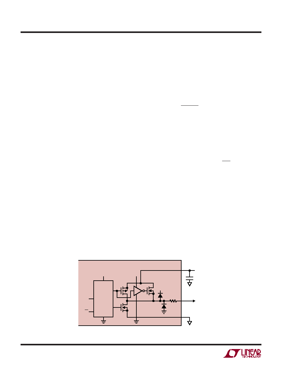
DIGITAL OUTPUTS
Digital Output Buffers
Figure 9 shows an equivalent circuit for a single output
buffer. Each buffer is powered by OVDD and OGND, iso-
lated from the ADC power and ground. The additional
N-channel transistor in the output driver allows operation
down to low voltages. The internal resistor in series with
the output makes the output appear as 50
to external
circuitry and may eliminate the need for external damping
resistors.
Output Loading
As with all high speed/high resolution converters the
digital output loading can affect the performance. The
digital outputs of the LTC1747 should drive a minimal
capacitive load to avoid possible interaction between the
digital outputs and sensitive input circuitry. The output
should be buffered with a device such as an ALVCH16373
CMOS latch. For full speed operation the capacitive load
should be kept under 10pF. A resistor in series with the
APPLICATIO S I FOR ATIO
WU
UU
output may be used but is not required since the ADC has
a series resistor of 43
on chip.
Lower OVDD voltages will also help reduce interference
from the digital outputs.
Format
The LTC1747 parallel digital output can be selected for
offset binary or 2’s complement format. The format is
selected with the MSBINV pin; high selects offset binary.
Overflow Bit
An overflow output bit indicates when the converter is
overranged or underranged. When OF outputs a logic high
the converter is either overranged or underranged.
Output Clock
The ADC has a delayed version of the ENC input available
as a digital output, CLKOUT. The CLKOUT pin can be used
to synchronize the converter data to the digital system.
This is necessary when using a sinusoidal encode. Data
will be updated just after CLKOUT falls and can be latched
on the rising edge of CLKOUT.
Output Driver Power
Separate output power and ground pins allow the output
drivers to be isolated from the analog circuitry. The power
supply for the digital output buffers, OVDD, should be tied
to the same power supply as for the logic being driven. For
example if the converter is driving a DSP powered by a 3V
supply then OVDD should be tied to that same 3V supply.
LTC1747
1747 F09
OVDD
VDD
0.1
F
43
TYPICAL
DATA
OUTPUT
OGND
OVDD
0.5V TO
VDD
PREDRIVER
LOGIC
DATA
FROM
LATCH
OE
Figure 9. Equivalent Circuit for a Digital Output Buffer
相关PDF资料 |
PDF描述 |
|---|---|
| LTC1748CFW#TRPBF | IC ADC 14BIT 80MSPS 48-TSSOP |
| LTC1749IFW#PBF | IC ADC 12BIT 80MSPS SMPL 48TSSOP |
| LTC1750IFW#PBF | IC ADC 14BIT 80MSPS SMPL 48TSSOP |
| LTC1799HS5#TRPBF | IC OSC SILICON 33MHZ TSOT23-5 |
| LTC1821ACGW | IC D/A CONV 16BIT PRECISE 36SSOP |
相关代理商/技术参数 |
参数描述 |
|---|---|
| LTC1748CFW | 功能描述:IC ADC 14BIT 80MSPS 48-TSSOP RoHS:否 类别:集成电路 (IC) >> 数据采集 - 模数转换器 系列:- 标准包装:1 系列:- 位数:14 采样率(每秒):83k 数据接口:串行,并联 转换器数目:1 功率耗散(最大):95mW 电压电源:双 ± 工作温度:0°C ~ 70°C 安装类型:通孔 封装/外壳:28-DIP(0.600",15.24mm) 供应商设备封装:28-PDIP 包装:管件 输入数目和类型:1 个单端,双极 |
| LTC1748CFW#PBF | 功能描述:IC ADC 14BIT 80MSPS 48-TSSOP RoHS:是 类别:集成电路 (IC) >> 数据采集 - 模数转换器 系列:- 标准包装:1 系列:- 位数:14 采样率(每秒):83k 数据接口:串行,并联 转换器数目:1 功率耗散(最大):95mW 电压电源:双 ± 工作温度:0°C ~ 70°C 安装类型:通孔 封装/外壳:28-DIP(0.600",15.24mm) 供应商设备封装:28-PDIP 包装:管件 输入数目和类型:1 个单端,双极 |
| LTC1748CFW#TR | 功能描述:IC ADC SMPL 14BIT 80MSPS 48TSSOP RoHS:否 类别:集成电路 (IC) >> 数据采集 - 模数转换器 系列:- 标准包装:1 系列:- 位数:14 采样率(每秒):83k 数据接口:串行,并联 转换器数目:1 功率耗散(最大):95mW 电压电源:双 ± 工作温度:0°C ~ 70°C 安装类型:通孔 封装/外壳:28-DIP(0.600",15.24mm) 供应商设备封装:28-PDIP 包装:管件 输入数目和类型:1 个单端,双极 |
| LTC1748CFW#TRPBF | 功能描述:IC ADC 14BIT 80MSPS 48-TSSOP RoHS:是 类别:集成电路 (IC) >> 数据采集 - 模数转换器 系列:- 产品培训模块:Lead (SnPb) Finish for COTS Obsolescence Mitigation Program 标准包装:2,500 系列:- 位数:12 采样率(每秒):3M 数据接口:- 转换器数目:- 功率耗散(最大):- 电压电源:- 工作温度:- 安装类型:表面贴装 封装/外壳:SOT-23-6 供应商设备封装:SOT-23-6 包装:带卷 (TR) 输入数目和类型:- |
| LTC1748IFW | 功能描述:IC ADC SMPL 14BIT 80MSPS 48TSSOP RoHS:否 类别:集成电路 (IC) >> 数据采集 - 模数转换器 系列:- 标准包装:1 系列:- 位数:14 采样率(每秒):83k 数据接口:串行,并联 转换器数目:1 功率耗散(最大):95mW 电压电源:双 ± 工作温度:0°C ~ 70°C 安装类型:通孔 封装/外壳:28-DIP(0.600",15.24mm) 供应商设备封装:28-PDIP 包装:管件 输入数目和类型:1 个单端,双极 |
发布紧急采购,3分钟左右您将得到回复。