- 您现在的位置:买卖IC网 > PDF目录10531 > LTC1856CG#PBF (Linear Technology)IC ADC 16BIT 100KSPS 28-SSOP PDF资料下载
参数资料
| 型号: | LTC1856CG#PBF |
| 厂商: | Linear Technology |
| 文件页数: | 20/24页 |
| 文件大小: | 0K |
| 描述: | IC ADC 16BIT 100KSPS 28-SSOP |
| 标准包装: | 47 |
| 位数: | 16 |
| 采样率(每秒): | 100k |
| 数据接口: | MICROWIRE?,串行,SPI? |
| 转换器数目: | 1 |
| 功率耗散(最大): | 40mW |
| 电压电源: | 模拟和数字 |
| 工作温度: | 0°C ~ 70°C |
| 安装类型: | 表面贴装 |
| 封装/外壳: | 28-SSOP(0.209",5.30mm 宽) |
| 供应商设备封装: | 28-SSOP |
| 包装: | 管件 |
| 输入数目和类型: | 8 个单端,双极;4 个差分,双极 |
| 产品目录页面: | 1347 (CN2011-ZH PDF) |
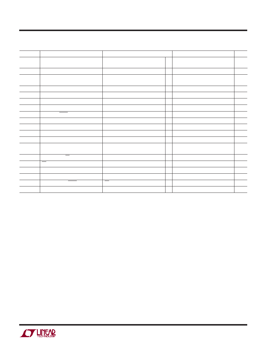
5
LTC1854/LTC1855/LTC1856
185456fa
The
● denotes the specifications which apply over the full operating temperature
range, otherwise specifications are at TA = 25
∞C. (Note 5)
TI I G CHARACTERISTICS
U
W
SYMBOL
PARAMETER
CONDITIONS
MIN
TYP
MAX
UNITS
fSAMPLE(MAX) Maximum Sampling Frequency
Through CH0 to CH7 Inputs
●
100
kHz
Through ADC+, ADC– Only
166
kHz
tCONV
Conversion Time
●
45
ms
tACQ
Acquisition Time
Through CH0 to CH7 Inputs
●
4
ms
Through ADC+, ADC– Only
1
ms
fSCK
SCK Frequency
(Note 13)
●
0
20
MHz
tr
SDO Rise Time
See Test Circuits
6
ns
tf
SDO Fall Time
See Test Circuits
6
ns
t1
CONVST High Time
●
40
ns
t2
CONVST to BUSY Delay
CL = 25pF, See Test Circuits
●
15
30
ns
t3
SCK Period
●
50
ns
t4
SCK High
●
10
ns
t5
SCK Low
●
10
ns
t6
Delay Time, SCK
to SDO Valid
CL = 25pF, See Test Circuits
●
25
45
ns
t7
Time from Previous SDO Data Remains
CL = 25pF, See Test Circuits
●
520
ns
Valid After SCK
t8
SDO Valid After RD
CL = 25pF, See Test Circuits
●
11
30
ns
t9
RD
to SCK Setup Time
●
20
ns
t10
SDI Setup Time Before SCK
≠
●
0ns
t11
SDI Hold Time After SCK
≠
●
7ns
t12
SDO Valid Before BUSY
≠
RD = Low, CL = 25pF, See Test Circuits
●
520
ns
t13
Bus Relinquish Time
See Test Circuits
●
10
30
ns
Note 1: Stresses beyond those listed under Absolute Maximum Ratings
may cause permanent damage to the device. Exposure to any Absolute
Maximum Rating condition for extended periods may affect device
reliability and lifetime.
Note 2: All voltage values are with respect to ground with DGND, AGND1,
AGND2 and AGND3 wired together unless otherwise noted.
Note 3: When these pin voltages are taken below ground or above AVDD =
DVDD = OVDD = VDD, they will be clamped by internal diodes. This product
can handle currents of greater than 100mA below ground or above VDD
without latchup.
Note 4: When these pin voltages are taken below ground they will be
clamped by internal diodes. This product can handle currents of greater
than 100mA below ground without latchup. These pins are not clamped
to VDD.
Note 5: VDD = 5V, fSAMPLE = 100kHz, tr = tf = 5ns unless otherwise
specified.
Note 6: Linearity, offset and full-scale specifications apply for a single-
ended analog MUX input with respect to ground or ADC+ with respect to
ADC– tied to ground.
Note 7: Integral nonlinearity is defined as the deviation of a code from a
straight line passing through the actual end points of the transfer curve.
The deviation is measured from the center of the quantization band.
Note 8: Bipolar zero error is the offset voltage measured from – 0.5LSB
when the output code flickers between 0000 0000 0000 0000 and 1111
1111 1111 1111 for the LTC1856, between 00 0000 0000 0000 and 11
1111 1111 1111 for the LTC1855 and between 0000 0000 0000 and 1111
1111 1111 for the LTC1854.
Note 9: Guaranteed by design, not subject to test.
Note 10: Recommended operating conditions.
Note 11: Full-scale bipolar error is the worst case of –FS or +FS
untrimmed deviation from ideal first and last code transitions, divided by
the full-scale range, and includes the effect of offset error.
Note 12: Recovers to specified performance after (2 FS) input
overvoltage.
Note 13: t6 of 45ns maximum allows fSCK up to 10MHz for rising capture
with 50% duty cycle and fSCK up to 20MHz for falling capture (with 5ns
setup time for the receiving logic).
相关PDF资料 |
PDF描述 |
|---|---|
| MS3102A24-16P | CONN RCPT 7POS BOX MNT W/PINS |
| VI-J42-MW-F1 | CONVERTER MOD DC/DC 15V 100W |
| LTC2351HUH-14#PBF | IC ADC 14BIT 1.5MSPS 32-QFN |
| MS3102C20-33P | CONN RCPT 11POS BOX MNT W/PINS |
| AD7892ARZ-2 | IC ADC 12BIT LP 500KSPS 24SOIC |
相关代理商/技术参数 |
参数描述 |
|---|---|
| LTC1856IG#PBF | 功能描述:IC ADC 16BIT 100KSPS 28-SSOP RoHS:是 类别:集成电路 (IC) >> 数据采集 - 模数转换器 系列:- 标准包装:1 系列:- 位数:14 采样率(每秒):83k 数据接口:串行,并联 转换器数目:1 功率耗散(最大):95mW 电压电源:双 ± 工作温度:0°C ~ 70°C 安装类型:通孔 封装/外壳:28-DIP(0.600",15.24mm) 供应商设备封装:28-PDIP 包装:管件 输入数目和类型:1 个单端,双极 |
| LTC1856IG#TRPBF | 功能描述:IC ADC 16BIT 100KSPS 28-SSOP RoHS:是 类别:集成电路 (IC) >> 数据采集 - 模数转换器 系列:- 标准包装:1,000 系列:- 位数:12 采样率(每秒):300k 数据接口:并联 转换器数目:1 功率耗散(最大):75mW 电压电源:单电源 工作温度:0°C ~ 70°C 安装类型:表面贴装 封装/外壳:24-SOIC(0.295",7.50mm 宽) 供应商设备封装:24-SOIC 包装:带卷 (TR) 输入数目和类型:1 个单端,单极;1 个单端,双极 |
| LTC1857CG | 制造商:Linear Technology 功能描述:ADC Single SAR 100ksps 12-bit Serial 28-Pin SSOP |
| LTC1857CG#PBF | 功能描述:IC ADC 8CH 12BIT 100KSPS 28-SSOP RoHS:是 类别:集成电路 (IC) >> 数据采集 - 模数转换器 系列:SoftSpan™ 标准包装:1 系列:microPOWER™ 位数:8 采样率(每秒):1M 数据接口:串行,SPI? 转换器数目:1 功率耗散(最大):- 电压电源:模拟和数字 工作温度:-40°C ~ 125°C 安装类型:表面贴装 封装/外壳:24-VFQFN 裸露焊盘 供应商设备封装:24-VQFN 裸露焊盘(4x4) 包装:Digi-Reel® 输入数目和类型:8 个单端,单极 产品目录页面:892 (CN2011-ZH PDF) 其它名称:296-25851-6 |
| LTC1857CG#PBF | 制造商:Linear Technology 功能描述:ADC, 8CH, 12BIT, 100KSPS, SSOP-28 |
发布紧急采购,3分钟左右您将得到回复。