- 您现在的位置:买卖IC网 > PDF目录44988 > LTC1871EMS#TR-1 (LINEAR TECHNOLOGY CORP) SWITCHING CONTROLLER, 1000 kHz SWITCHING FREQ-MAX, PDSO10 PDF资料下载
参数资料
| 型号: | LTC1871EMS#TR-1 |
| 厂商: | LINEAR TECHNOLOGY CORP |
| 元件分类: | 稳压器 |
| 英文描述: | SWITCHING CONTROLLER, 1000 kHz SWITCHING FREQ-MAX, PDSO10 |
| 封装: | PLASTIC, MSOP-10 |
| 文件页数: | 16/36页 |
| 文件大小: | 354K |
| 代理商: | LTC1871EMS#TR-1 |
第1页第2页第3页第4页第5页第6页第7页第8页第9页第10页第11页第12页第13页第14页第15页当前第16页第17页第18页第19页第20页第21页第22页第23页第24页第25页第26页第27页第28页第29页第30页第31页第32页第33页第34页第35页第36页
23
LTC1871-1
18711fa
2. Beware of ground loops in multiple layer PC boards. Try
to maintain one central ground node on the board and
use the input capacitor to avoid excess input ripple for
high output current power supplies. If the ground plane
is to be used for high DC currents, choose a path away
from the small-signal components.
3. Place the CVCC capacitor immediately adjacent to the
INTVCC and GND pins on the IC package. This capacitor
carries high di/dt MOSFET gate drive currents. A low
ESR and ESL 4.7
μF ceramic capacitor works well here.
4. The high di/dt loop from the bottom terminal of the
output capacitor, through the power MOSFET, through
the boost diode and back through the output capacitors
should be kept as tight as possible to reduce inductive
ringing. Excess inductance can cause increased stress
on the power MOSFET and increase HF noise on the
output. If low ESR ceramic capacitors are used on the
output to reduce output noise, place these capacitors
close to the boost diode in order to keep the series
inductance to a minimum.
5. Check the stress on the power MOSFET by measuring
its drain-to-source voltage directly across the device
terminals (reference the ground of a single scope probe
directly to the source pad on the PC board). Beware of
inductive ringing which can exceed the maximum speci-
fied voltage rating of the MOSFET. If this ringing cannot
be avoided and exceeds the maximum rating of the
device, either choose a higher voltage device or specify
an avalanche-rated power MOSFET. Not all MOSFETs
are created equal (some are more equal than others).
6. Place the small-signal components away from high
frequency switching nodes. In the layout shown in
Figure 14, all of the small-signal components have been
placed on one side of the IC and all of the power
components have been placed on the other. This also
allows the use of a pseudo-Kelvin connection for the
signal ground, where high di/dt gate driver currents
flow out of the IC ground pin in one direction (to the
bottom plate of the INTVCC decoupling capacitor) and
small-signal currents flow in the other direction.
7. If a sense resistor is used in the source of the power
MOSFET, minimize the capacitance between the SENSE
pin trace and any high frequency switching nodes. The
LTC1871-1 contains an internal leading edge blanking
time of approximately 180ns, which should be ad-
equate for most applications.
8. For optimum load regulation and true remote sensing,
the top of the output resistor divider should connect
independently to the top of the output capacitor (Kelvin
connection), staying away from any high dV/dt traces.
Place the divider resistors near the LTC1871-1 in order
to keep the high impedance FB node short.
9. For applications with multiple switching power con-
verters connected to the same input supply, make sure
that the input filter capacitor for the LTC1871-1 is not
shared with other converters. AC input current from
another converter could cause substantial input voltage
ripple, and this could interfere with the operation of the
LTC1871-1. A few inches of PC trace or wire (L
≈
100nH) between the CIN of the LTC1871-1 and the
actual source VIN should be sufficient to prevent current
sharing problems.
APPLICATIO S I FOR ATIO
WU
UU
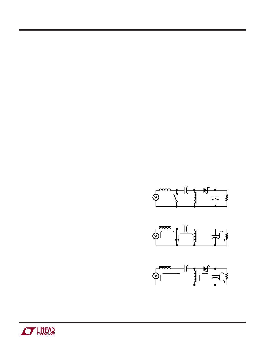
Figures 16. SEPIC Topology and Current Flow
+
SW
L2
COUT
RL
VOUT
VIN
C1
D1
L1
16a. SEPIC Topology
+
RL
VOUT
VIN
D1
16c. Current Flow During Switch Off-Time
+
RL
VOUT
VIN
16b. Current Flow During Switch On-Time
相关PDF资料 |
PDF描述 |
|---|---|
| LTC1871IMS#TRPBF-1 | SWITCHING CONTROLLER, 1000 kHz SWITCHING FREQ-MAX, PDSO10 |
| LTC1871HMS#TR | 0.05 A SWITCHING CONTROLLER, 1000 kHz SWITCHING FREQ-MAX, PDSO10 |
| LTC1871HMS | 0.05 A SWITCHING CONTROLLER, 1000 kHz SWITCHING FREQ-MAX, PDSO10 |
| LTC1877IMS8#TRPBF | 1.5 A SWITCHING REGULATOR, 605 kHz SWITCHING FREQ-MAX, PDSO8 |
| LTC1929IG-PG | 3 A DUAL SWITCHING CONTROLLER, 310 kHz SWITCHING FREQ-MAX, PDSO28 |
相关代理商/技术参数 |
参数描述 |
|---|---|
| LTC1871HMS#PBF | 功能描述:IC REG CTRLR BST FLYBK CM 10MSOP RoHS:是 类别:集成电路 (IC) >> PMIC - 稳压器 - DC DC 切换控制器 系列:- 标准包装:2,500 系列:- PWM 型:电流模式 输出数:1 频率 - 最大:500kHz 占空比:96% 电源电压:4 V ~ 36 V 降压:无 升压:是 回扫:无 反相:无 倍增器:无 除法器:无 Cuk:无 隔离:无 工作温度:-40°C ~ 125°C 封装/外壳:24-WQFN 裸露焊盘 包装:带卷 (TR) |
| LTC1871HMS#TRPBF | 功能描述:IC REG CTRLR BST FLYBK CM 10MSOP RoHS:是 类别:集成电路 (IC) >> PMIC - 稳压器 - DC DC 切换控制器 系列:- 标准包装:2,500 系列:- PWM 型:电流模式 输出数:1 频率 - 最大:500kHz 占空比:96% 电源电压:4 V ~ 36 V 降压:无 升压:是 回扫:无 反相:无 倍增器:无 除法器:无 Cuk:无 隔离:无 工作温度:-40°C ~ 125°C 封装/外壳:24-WQFN 裸露焊盘 包装:带卷 (TR) |
| LTC1871HMSPBF | 制造商:Linear Technology 功能描述:PWM Controller Current Mode MSOP10 |
| LTC1871IMS | 功能描述:IC REG CTRLR BST FLYBK CM 10MSOP RoHS:否 类别:集成电路 (IC) >> PMIC - 稳压器 - DC DC 切换控制器 系列:- 标准包装:2,500 系列:- PWM 型:电流模式 输出数:1 频率 - 最大:500kHz 占空比:96% 电源电压:4 V ~ 36 V 降压:无 升压:是 回扫:无 反相:无 倍增器:无 除法器:无 Cuk:无 隔离:无 工作温度:-40°C ~ 125°C 封装/外壳:24-WQFN 裸露焊盘 包装:带卷 (TR) |
| LTC1871IMS#PBF | 功能描述:IC REG CTRLR BST FLYBK CM 10MSOP RoHS:是 类别:集成电路 (IC) >> PMIC - 稳压器 - DC DC 切换控制器 系列:- 标准包装:2,500 系列:- PWM 型:电流模式 输出数:1 频率 - 最大:500kHz 占空比:96% 电源电压:4 V ~ 36 V 降压:无 升压:是 回扫:无 反相:无 倍增器:无 除法器:无 Cuk:无 隔离:无 工作温度:-40°C ~ 125°C 封装/外壳:24-WQFN 裸露焊盘 包装:带卷 (TR) |
发布紧急采购,3分钟左右您将得到回复。