- 您现在的位置:买卖IC网 > PDF目录44988 > LTC1871HMS (LINEAR TECHNOLOGY CORP) 0.05 A SWITCHING CONTROLLER, 1000 kHz SWITCHING FREQ-MAX, PDSO10 PDF资料下载
参数资料
| 型号: | LTC1871HMS |
| 厂商: | LINEAR TECHNOLOGY CORP |
| 元件分类: | 稳压器 |
| 英文描述: | 0.05 A SWITCHING CONTROLLER, 1000 kHz SWITCHING FREQ-MAX, PDSO10 |
| 封装: | PLASTIC, MSOP-10 |
| 文件页数: | 7/36页 |
| 文件大小: | 519K |
| 代理商: | LTC1871HMS |
第1页第2页第3页第4页第5页第6页当前第7页第8页第9页第10页第11页第12页第13页第14页第15页第16页第17页第18页第19页第20页第21页第22页第23页第24页第25页第26页第27页第28页第29页第30页第31页第32页第33页第34页第35页第36页
LTC1871
15
1871fe
APPLICATIONS INFORMATION
Boost Converter: Inductor Core Selection
Once the value for L is known, the type of inductor must
be selected. High efciency converters generally cannot
afford the core loss found in low cost powdered iron cores,
forcing the use of more expensive ferrite, molypermalloy
or Kool Mμ cores. Actual core loss is independent of core
size for a xed inductor value, but is very dependent on
the inductance selected. As inductance increases, core
losses go down. Unfortunately, increased inductance
requires more turns of wire and therefore, copper losses
will increase. Generally, there is a tradeoff between core
losses and copper losses that needs to be balanced.
Ferrite designs have very low core losses and are pre-
ferred at high switching frequencies, so design goals can
concentrate on copper losses and preventing saturation.
Ferrite core material saturates “hard,” meaning that the
inductance collapses rapidly when the peak design current
is exceeded. This results in an abrupt increase in inductor
ripple current and consequently, output voltage ripple. Do
not allow the core to saturate!
Molypermalloy (from Magnetics, Inc.) is a very good,
low cost core material for toroids, but is more expensive
than ferrite. A reasonable compromise from the same
manufacturer is Kool Mμ.
Boost Converter: Power MOSFET Selection
The power MOSFET serves two purposes in the LTC1871:
it represents the main switching element in the power path,
and its RDS(ON) represents the current sensing element
for the control loop. Important parameters for the power
MOSFET include the drain-to-source breakdown voltage
(BVDSS), the threshold voltage (VGS(TH)), the on-resistance
(RDS(ON))versusgate-to-sourcevoltage,thegate-to-source
and gate-to-drain charges (QGS and QGD, respectively),
the maximum drain current (ID(MAX)) and the MOSFET’s
thermal resistances (RTH(JC) and RTH(JA)).
The gate drive voltage is set by the 5.2V INTVCC low drop
regulator. Consequently, logic-level threshold MOSFETs
should be used in most LTC1871 applications. If low input
voltage operation is expected (e.g., supplying power from
a lithium-ion battery or a 3.3V logic supply), then sublogic-
level threshold MOSFETs should be used.
Pay close attention to the BVDSS specications for the
MOSFETs relative to the maximum actual switch voltage in
the application. Many logic-level devices are limited to 30V
or less, and the switch node can ring during the turn-off of
the MOSFET due to layout parasitics. Check the switching
waveforms of the MOSFET directly across the drain and
source terminals using the actual PC board layout (not
just on a lab breadboard!) for excessive ringing.
During the switch on-time, the control circuit limits the
maximum voltage drop across the power MOSFET to about
150mV (at low duty cycle). The peak inductor current
is therefore limited to 150mV/RDS(ON). The relationship
between the maximum load current, duty cycle and the
RDS(ON) of the power MOSFET is:
RDS(ON) VSENSE(MAX)
1– DMAX
1
+
2
IO(MAX) T
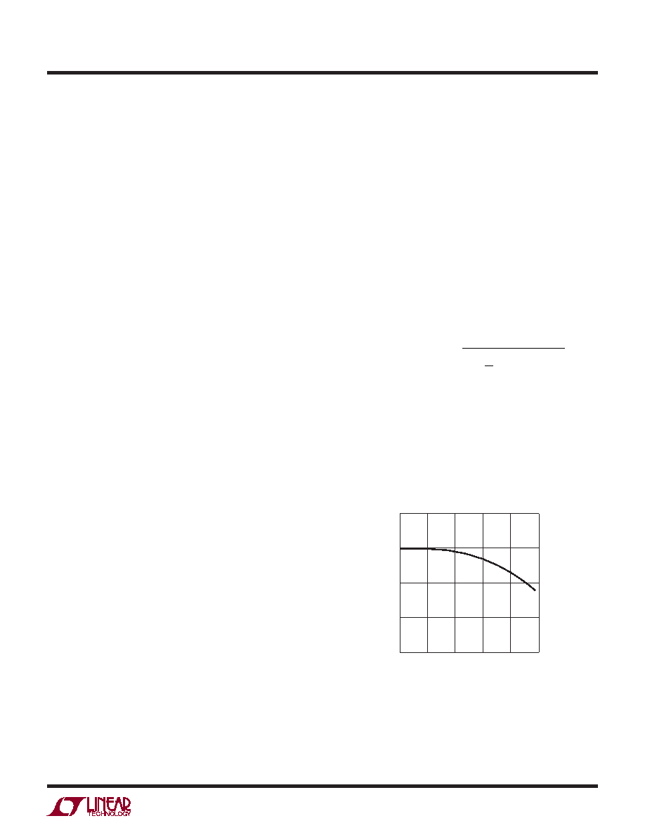
The VSENSE(MAX) term is typically 150mV at low duty
cycle, and is reduced to about 100mV at a duty cycle of
92% due to slope compensation, as shown in Figure 10.
The ρT term accounts for the temperature coefcient of
the RDS(ON) of the MOSFET, which is typically 0.4%/°C.
Figure 11 illustrates the variation of normalized RDS(ON)
over temperature for a typical power MOSFET.
DUTY CYCLE
0
MAXIMUM
CURRENT
SENSE
VOLTAGE
(mV)
100
150
0.8
1871 F10
50
0
0.2
0.4
0.5
1.0
200
Figure 10. Maximum SENSE Threshold Voltage vs Duty Cycle
相关PDF资料 |
PDF描述 |
|---|---|
| LTC1877IMS8#TRPBF | 1.5 A SWITCHING REGULATOR, 605 kHz SWITCHING FREQ-MAX, PDSO8 |
| LTC1929IG-PG | 3 A DUAL SWITCHING CONTROLLER, 310 kHz SWITCHING FREQ-MAX, PDSO28 |
| LTC203MJ/883B | QUAD 1-CHANNEL, SGL POLE SGL THROW SWITCH, CDIP16 |
| LTC202MJ/883B | QUAD 1-CHANNEL, SGL POLE SGL THROW SWITCH, CDIP16 |
| LTC201AMJ/883B | QUAD 1-CHANNEL, SGL POLE SGL THROW SWITCH, CDIP16 |
相关代理商/技术参数 |
参数描述 |
|---|---|
| LTC1871HMS#PBF | 功能描述:IC REG CTRLR BST FLYBK CM 10MSOP RoHS:是 类别:集成电路 (IC) >> PMIC - 稳压器 - DC DC 切换控制器 系列:- 标准包装:2,500 系列:- PWM 型:电流模式 输出数:1 频率 - 最大:500kHz 占空比:96% 电源电压:4 V ~ 36 V 降压:无 升压:是 回扫:无 反相:无 倍增器:无 除法器:无 Cuk:无 隔离:无 工作温度:-40°C ~ 125°C 封装/外壳:24-WQFN 裸露焊盘 包装:带卷 (TR) |
| LTC1871HMS#TRPBF | 功能描述:IC REG CTRLR BST FLYBK CM 10MSOP RoHS:是 类别:集成电路 (IC) >> PMIC - 稳压器 - DC DC 切换控制器 系列:- 标准包装:2,500 系列:- PWM 型:电流模式 输出数:1 频率 - 最大:500kHz 占空比:96% 电源电压:4 V ~ 36 V 降压:无 升压:是 回扫:无 反相:无 倍增器:无 除法器:无 Cuk:无 隔离:无 工作温度:-40°C ~ 125°C 封装/外壳:24-WQFN 裸露焊盘 包装:带卷 (TR) |
| LTC1871HMSPBF | 制造商:Linear Technology 功能描述:PWM Controller Current Mode MSOP10 |
| LTC1871IMS | 功能描述:IC REG CTRLR BST FLYBK CM 10MSOP RoHS:否 类别:集成电路 (IC) >> PMIC - 稳压器 - DC DC 切换控制器 系列:- 标准包装:2,500 系列:- PWM 型:电流模式 输出数:1 频率 - 最大:500kHz 占空比:96% 电源电压:4 V ~ 36 V 降压:无 升压:是 回扫:无 反相:无 倍增器:无 除法器:无 Cuk:无 隔离:无 工作温度:-40°C ~ 125°C 封装/外壳:24-WQFN 裸露焊盘 包装:带卷 (TR) |
| LTC1871IMS#PBF | 功能描述:IC REG CTRLR BST FLYBK CM 10MSOP RoHS:是 类别:集成电路 (IC) >> PMIC - 稳压器 - DC DC 切换控制器 系列:- 标准包装:2,500 系列:- PWM 型:电流模式 输出数:1 频率 - 最大:500kHz 占空比:96% 电源电压:4 V ~ 36 V 降压:无 升压:是 回扫:无 反相:无 倍增器:无 除法器:无 Cuk:无 隔离:无 工作温度:-40°C ~ 125°C 封装/外壳:24-WQFN 裸露焊盘 包装:带卷 (TR) |
发布紧急采购,3分钟左右您将得到回复。