- 您现在的位置:买卖IC网 > PDF目录14072 > LTC1878EMS8#TR (Linear Technology)IC REG BUCK SYNC ADJ 0.6A 8MSOP PDF资料下载
参数资料
| 型号: | LTC1878EMS8#TR |
| 厂商: | Linear Technology |
| 文件页数: | 11/16页 |
| 文件大小: | 0K |
| 描述: | IC REG BUCK SYNC ADJ 0.6A 8MSOP |
| 标准包装: | 2,500 |
| 类型: | 降压(降压) |
| 输出类型: | 可调式 |
| 输出数: | 1 |
| 输出电压: | 0.8 V ~ 6 V |
| 输入电压: | 2.65 V ~ 6 V |
| PWM 型: | 电流模式,混合 |
| 频率 - 开关: | 550kHz |
| 电流 - 输出: | 600mA |
| 同步整流器: | 是 |
| 工作温度: | -40°C ~ 85°C |
| 安装类型: | 表面贴装 |
| 封装/外壳: | 8-TSSOP,8-MSOP(0.118",3.00mm 宽) |
| 包装: | 带卷 (TR) |
| 供应商设备封装: | 8-MSOP |
| 其它名称: | LTC1878EMS8TR |
�� �
�
�LTC1878�
�APPLICATIO� S� I� FOR� ATIO�
�external� and� internal� frequencies� are� the� same� but� exhibit�
�a� phase� difference,� the� current� sources� turn� on� for� an�
�amount� of� time� corresponding� to� the� phase� difference.�
�Thus� the� voltage� on� the� PLL� LPF� pin� is� adjusted� until� the�
�phase� and� frequency� of� the� external� and� internal� oscilla-�
�tors� are� identical.� At� this� stable� operating� point� the� phase�
�comparator� output� is� high� impedance� and� the� filter�
�capacitor� C� LP� holds� the� voltage.�
�1�
�0.1�
�0.01�
�0.001�
�0.0001�
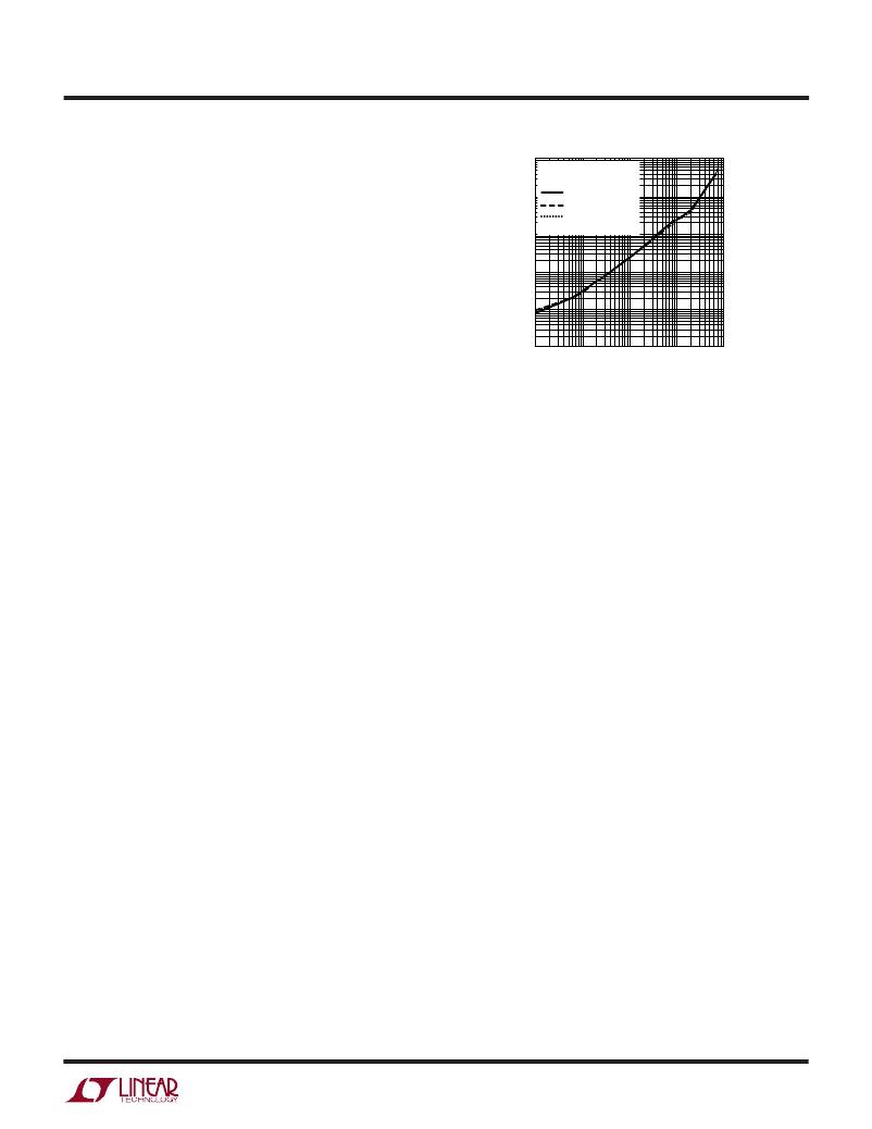
�V� IN� =� 4.2V�
�L� =� 10� μ� H�
�V� OUT� =� 1.5V�
�V� OUT� =� 2.5V�
�V� OUT� =� 3.3V�
�Burst� Mode� OPERATION�
�The� loop� filter� components� C� LP� and� R� LP� smooth� out� the�
�current� pulses� from� the� phase� detector� and� provide� a�
�0.00001�
�0.1�
�1�
�10� 100�
�1000�
�stable� input� to� the� voltage� controlled� oscillator.� The� filter�
�component’s� C� LP� and� R� LP� determine� how� fast� the� loop�
�acquires� lock.� Typically� R� LP� =� 10k� and� C� LP� is� 2200pF� to�
�0.01� μ� F.� When� not� synchronized� to� an� external� clock,� the�
�internal� connection� to� the� VCO� is� disconnected.� This�
�disallows� setting� the� internal� oscillator� frequency� by� a� DC�
�voltage� on� the� V� PLL� LPF� pin.�
�Efficiency� Considerations�
�The� efficiency� of� a� switching� regulator� is� equal� to� the�
�output� power� divided� by� the� input� power� times� 100%.� It� is�
�often� useful� to� analyze� individual� losses� to� determine� what�
�is� limiting� the� efficiency� and� which� change� would� produce�
�the� most� improvement.� Efficiency� can� be� expressed� as:�
�Efficiency� =� 100%� –� (L1� +� L2� +� L3� +� ...)�
�where� L1,� L2,� etc.� are� the� individual� losses� as� a� percentage�
�of� input� power.�
�Although� all� dissipative� elements� in� the� circuit� produce�
�losses,� two� main� sources� usually� account� for� most� of� the�
�losses� in� LTC1878� circuits:� V� IN� quiescent� current� and� I� 2� R�
�losses.� The� V� IN� quiescent� current� loss� dominates� the�
�efficiency� loss� at� very� low� load� currents� whereas� the� I� 2� R�
�loss� dominates� the� efficiency� loss� at� medium� to� high� load�
�currents.� In� a� typical� efficiency� plot,� the� efficiency� curve� at�
�very� low� load� currents� can� be� misleading� since� the� actual�
�power� lost� is� of� no� consequence� as� illustrated� in� Figure� 6.�
�1.� The� V� IN� quiescent� current� is� due� to� two� components:�
�the� DC� bias� current� as� given� in� the� electrical� character-�
�istics� and� the� internal� main� switch� and� synchronous�
�switch� gate� charge� currents.� The� gate� charge� current�
�results� from� switching� the� gate� capacitance� of� the�
�LOAD� CURRENT� (mA)�
�1878� F06�
�Figure� 6.� Power� Lost� vs� Load� Current�
�internal� power� MOSFET� switches.� Each� time� the� gate� is�
�switched� from� high� to� low� to� high� again,� a� packet� of�
�charge� dQ� moves� from� V� IN� to� ground.� The� resulting�
�dQ/dt� is� the� current� out� of� V� IN� that� is� typically� larger� than�
�the� DC� bias� current.� In� continuous� mode,� I� GATECHG� =�
�f(Q� T� +� Q� B� )� where� Q� T� and� Q� B� are� the� gate� charges� of� the�
�internal� top� and� bottom� switches.� Both� the� DC� bias� and�
�gate� charge� losses� are� proportional� to� V� IN� and� thus�
�their� effects� will� be� more� pronounced� at� higher� supply�
�voltages.�
�2.� I� 2� R� losses� are� calculated� from� the� resistances� of� the�
�internal� switches,� R� SW� ,� and� external� inductor� R� L� .� In�
�continuous� mode� the� average� output� current� flowing�
�through� inductor� L� is� “chopped”� between� the� main�
�switch� and� the� synchronous� switch.� Thus,� the� series�
�resistance� looking� into� the� SW� pin� is� a� function� of� both�
�top� and� bottom� MOSFET� R� DS(ON)� and� the� duty� cycle�
�(DC)� as� follows:�
�R� SW� =� (R� DS(ON)TOP� )(DC)� +� (R� DS(ON)BOT� )(1� –� DC)�
�The� R� DS(ON)� for� both� the� top� and� bottom� MOSFETs� can�
�be� obtained� from� the� Typical� Performance� Charateristics�
�curves.� Thus,� to� obtain� I� 2� R� losses,� simply� add� R� SW� to�
�R� L� and� multiply� the� result� by� the� square� of� the� average�
�output� current.�
�Other� losses� including� C� IN� and� C� OUT� ESR� dissipative�
�losses� and� inductor� core� losses� generally� account� for� less�
�than� 2%� total� additional� loss.�
�11�
�相关PDF资料 |
PDF描述 |
|---|---|
| 35PK33MEFC5X11 | CAP ALUM 33UF 35V 20% RADIAL |
| GBC30DRAN-S734 | CONN EDGECARD 60POS .100 R/A SLD |
| GBC30DRAH-S734 | CONN EDGECARD 60POS .100 R/A SLD |
| LT1676CS8 | IC REG BUCK ADJ 0.7A 8SOIC |
| LT1111CS8-12#TRPBF | IC REG BUCK BOOST INV 12V 8SOIC |
相关代理商/技术参数 |
参数描述 |
|---|---|
| LTC1878EMS8TRPBF | 制造商:Linear Technology 功能描述: |
| LTC1879EGN | 功能描述:IC REG BUCK SYNC ADJ 1.2A 16SSOP RoHS:否 类别:集成电路 (IC) >> PMIC - 稳压器 - DC DC 开关稳压器 系列:- 标准包装:2,500 系列:- 类型:降压(降压) 输出类型:固定 输出数:1 输出电压:1.2V,1.5V,1.8V,2.5V 输入电压:2.7 V ~ 20 V PWM 型:- 频率 - 开关:- 电流 - 输出:50mA 同步整流器:是 工作温度:-40°C ~ 125°C 安装类型:表面贴装 封装/外壳:10-TFSOP,10-MSOP(0.118",3.00mm 宽)裸露焊盘 包装:带卷 (TR) 供应商设备封装:10-MSOP 裸露焊盘 |
| LTC1879EGN#PBF | 功能描述:IC REG BUCK SYNC ADJ 1.2A 16SSOP RoHS:是 类别:集成电路 (IC) >> PMIC - 稳压器 - DC DC 开关稳压器 系列:- 标准包装:250 系列:- 类型:降压(降压) 输出类型:固定 输出数:1 输出电压:1.2V 输入电压:2.05 V ~ 6 V PWM 型:电压模式 频率 - 开关:2MHz 电流 - 输出:500mA 同步整流器:是 工作温度:-40°C ~ 85°C 安装类型:表面贴装 封装/外壳:6-UFDFN 包装:带卷 (TR) 供应商设备封装:6-SON(1.45x1) 产品目录页面:1032 (CN2011-ZH PDF) 其它名称:296-25628-2 |
| LTC1879EGN#TR | 功能描述:IC REG BUCK SYNC ADJ 1.2A 16SSOP RoHS:否 类别:集成电路 (IC) >> PMIC - 稳压器 - DC DC 开关稳压器 系列:- 标准包装:2,500 系列:- 类型:降压(降压) 输出类型:固定 输出数:1 输出电压:1.2V,1.5V,1.8V,2.5V 输入电压:2.7 V ~ 20 V PWM 型:- 频率 - 开关:- 电流 - 输出:50mA 同步整流器:是 工作温度:-40°C ~ 125°C 安装类型:表面贴装 封装/外壳:10-TFSOP,10-MSOP(0.118",3.00mm 宽)裸露焊盘 包装:带卷 (TR) 供应商设备封装:10-MSOP 裸露焊盘 |
| LTC1879EGN#TRPBF | 功能描述:IC REG BUCK SYNC ADJ 1.2A 16SSOP RoHS:是 类别:集成电路 (IC) >> PMIC - 稳压器 - DC DC 开关稳压器 系列:- 标准包装:2,500 系列:- 类型:降压(降压) 输出类型:固定 输出数:1 输出电压:1.2V,1.5V,1.8V,2.5V 输入电压:2.7 V ~ 20 V PWM 型:- 频率 - 开关:- 电流 - 输出:50mA 同步整流器:是 工作温度:-40°C ~ 125°C 安装类型:表面贴装 封装/外壳:10-TFSOP,10-MSOP(0.118",3.00mm 宽)裸露焊盘 包装:带卷 (TR) 供应商设备封装:10-MSOP 裸露焊盘 |
发布紧急采购,3分钟左右您将得到回复。