参数资料
| 型号: | LTC2050HVCS5#TRM |
| 厂商: | Linear Technology |
| 文件页数: | 13/16页 |
| 文件大小: | 0K |
| 描述: | IC OPAMP ZERO-DRIFT TSOT23-5 |
| 标准包装: | 1 |
| 放大器类型: | 断路器(零漂移) |
| 电路数: | 1 |
| 输出类型: | 满摆幅 |
| 转换速率: | 2 V/µs |
| 增益带宽积: | 3MHz |
| 电流 - 输入偏压: | 25pA |
| 电压 - 输入偏移: | 0.5µV |
| 电流 - 电源: | 1mA |
| 电压 - 电源,单路/双路(±): | 2.7 V ~ 11 V,±1.35 V ~ 5.5 V |
| 工作温度: | 0°C ~ 70°C |
| 安装类型: | 表面贴装 |
| 封装/外壳: | SOT-23-5 细型,TSOT-23-5 |
| 供应商设备封装: | TSOT-23-5 |
| 包装: | 标准包装 |
| 产品目录页面: | 1321 (CN2011-ZH PDF) |
| 其它名称: | LTC2050HVCS5#TRMDKR |
LTC2050/LTC2050HV
6
2050fc
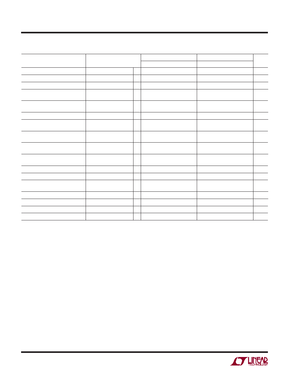
ELECTRICAL CHARACTERISTICS (LTC2050HV) The l denotes the specications which apply over the full
operating temperature range, otherwise specications are at TA = 25°C. VS = ±5V unless otherwise noted. (Note 3)
PARAMETER
CONDITIONS
C, I SUFFIXES
H SUFFIX
UNITS
MIN
TYP
MAX
MIN
TYP
MAX
Input Offset Voltage
(Note 2)
±0.5
±3
±0.5
±3
μV
Average Input Offset Drift
(Note 2)
l
±0.03
±0.05
μV/°C
Long-Term Offset Drift
50
nV/√mo
Input Bias Current (Note 4)
l
±25
±125
±300
±25
±125
±4000
pA
Input Offset Current (Note 4)
l
±250
±500
±250
±1000
pA
Input Noise Voltage
RS = 100Ω, 0.01Hz to 10Hz
1.5
μVP-P
Common Mode Rejection Ratio
VCM = V– to (V+ – 1.3)
l
120
115
130
120
115
130
dB
Power Supply Rejection Ratio
VS = 2.7V to 11V
l
120
115
130
120
115
130
dB
Large-Signal Voltage Gain
RL = 10k
125
120
140
125
120
140
dB
Maximum Output Voltage Swing
RL = 2k to GND
RL = 10k to GND
l
±4.75
±4.90
±4.94
±4.98
±4.50
±4.85
±4.94
±4.98
V
Slew Rate
2
V/μs
Gain Bandwidth Product
3
MHz
Supply Current
VSHDN = VIH, No Load
VSHDN = VIL
l
1
1.5
25
1
1.6
25
mA
μA
Shutdown Pin Input Low Voltage (VIL)
l
V– + 0.5
V
Shutdown Pin Input High Voltage (VIH)
l
V+ – 0.5
V
Shutdown Pin Input Current
VSHDN = V–
l
–3
–20
–3
–20
μA
Internal Sampling Frequency
7.5
kHz
Note 1: Stresses beyond those listed under Absolute Maximum Ratings
may cause permanent damage to the device. Exposure to any Absolute
Maximum Rating condition for extended periods may affect device
reliability and lifetime.
Note 2: These parameters are guaranteed by design. Thermocouple effects
preclude measurements of these voltage levels during automated testing.
Note 3: All versions of the LTC2050 are designed, characterized and
expected to meet the extended temperature limits of – 40°C and 125°C.
The LTC2050C/LTC2050HVC are guaranteed to meet the temperature limits
of 0°C and 70°C. The LTC2050I/LTC2050HVI are guaranteed to meet the
temperature limits of –40°C and 85°C. The LTC2050H/LTC2050HVH are
guaranteed to meet the temperature limits of –40°C and 125°C.
Note 4: The bias current measurement accuracy depends on the proximity
of the supply bypass capacitor to the device under test, especially at ±5V
supplies. Because of testing limitations on the placement of this bypass
capacitor, the bias current at ±5V supplies is guaranteed by design to meet
the data sheet limits, but tested to relaxed limits.
相关PDF资料 |
PDF描述 |
|---|---|
| TSW-134-26-G-S | CONN HEADER 34POS .100" SGL GOLD |
| AC0603FR-07180KL | RES 180K OHM 1/10W 1% 0603 |
| TSW-141-17-G-S | CONN HEADER 41POS .100" SGL GOLD |
| 5-102699-5 | 12 MODII HDR DRST SHRD A/PIN |
| MAX4377TASA+ | IC AMP CURRENT DUAL 8-SOIC |
相关代理商/技术参数 |
参数描述 |
|---|---|
| LTC2050HVCS5TRMPBF | 制造商:Linear Technology 功能描述:Op Amp GP RRO +/-5.5V/11V TSOT23-5 |
| LTC2050HVCS5-TRPBF | 制造商:LINER 制造商全称:Linear Technology 功能描述:Zero-Drift Operational Amplifi ers in SOT-23 |
| LTC2050HVCS6 | 制造商:Linear Technology 功能描述:SP Amp Zero Drift Amplifier Single R-R O/P ±5.5V/11V 6-Pin TSOT-23 |
| LTC2050HVCS6#PBF | 制造商:Linear Technology 功能描述:OP-AMP ZERO DRIFT 3MHZ 2V/u 制造商:Linear Technology 功能描述:OP-AMP, ZERO DRIFT, 3MHZ, 2V/us, TSOT-23-6; Op Amp Type:Zero Drift; No. of Amplifiers:1; Slew Rate:2V/s; Supply Voltage Range:2.7V to 5.5V; Amplifier Case Style:TSOT-23; No. of Pins:6; Bandwidth:3MHz; Operating Temperature Min:0C;RoHS Compliant: Yes |
| LTC2050HVCS6#TR | 功能描述:IC OPAMP ZERO DRIFT HV SOT23-6 RoHS:否 类别:集成电路 (IC) >> Linear - Amplifiers - Instrumentation 系列:- 标准包装:1,000 系列:- 放大器类型:电压反馈 电路数:4 输出类型:满摆幅 转换速率:33 V/µs 增益带宽积:20MHz -3db带宽:30MHz 电流 - 输入偏压:2nA 电压 - 输入偏移:3000µV 电流 - 电源:2.5mA 电流 - 输出 / 通道:30mA 电压 - 电源,单路/双路(±):4.5 V ~ 16.5 V,±2.25 V ~ 8.25 V 工作温度:-40°C ~ 85°C 安装类型:表面贴装 封装/外壳:14-SOIC(0.154",3.90mm 宽) 供应商设备封装:14-SOIC 包装:带卷 (TR) |
发布紧急采购,3分钟左右您将得到回复。