- 您现在的位置:买卖IC网 > PDF目录10105 > LTC2141IUP-14#TRPBF (Linear Technology)IC ADC DUAL 14BIT 65 MSPS 64-QFN PDF资料下载
参数资料
| 型号: | LTC2141IUP-14#TRPBF |
| 厂商: | Linear Technology |
| 文件页数: | 18/38页 |
| 文件大小: | 0K |
| 描述: | IC ADC DUAL 14BIT 65 MSPS 64-QFN |
| 标准包装: | 2,000 |
| 位数: | 14 |
| 采样率(每秒): | 40M |
| 数据接口: | 并联,串行,SPI |
| 转换器数目: | 2 |
| 功率耗散(最大): | 218mW |
| 电压电源: | 模拟和数字 |
| 工作温度: | -40°C ~ 85°C |
| 安装类型: | 表面贴装 |
| 封装/外壳: | 64-WFQFN 裸露焊盘 |
| 供应商设备封装: | 64-QFN(9x9) |
| 包装: | 带卷 (TR) |
| 输入数目和类型: | 2 个差分 |
| 配用: | DC890B-ND - BOARD USB DATA COLLECTION |
第1页第2页第3页第4页第5页第6页第7页第8页第9页第10页第11页第12页第13页第14页第15页第16页第17页当前第18页第19页第20页第21页第22页第23页第24页第25页第26页第27页第28页第29页第30页第31页第32页第33页第34页第35页第36页第37页第38页
25
21421014fa
LTC2142-14/
LTC2141-14/LTC2140-14
APPLICATIONS INFORMATION
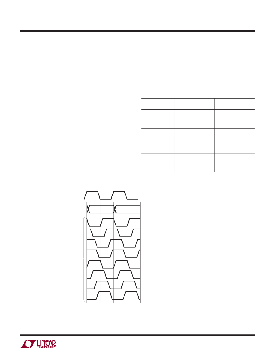
Phase Shifting the Output Clock
In full rate CMOS mode the data output bits normally
change at the same time as the falling edge of CLKOUT+,
so the rising edge of CLKOUT+ can be used to latch the
output data. In double data rate CMOS and LVDS modes
the data output bits normally change at the same time as
the falling and rising edges of CLKOUT+. To allow adequate
set-up and hold time when latching the data, the CLKOUT+
signal may need to be phase shifted relative to the data
output bits. Most FPGAs have this feature; this is generally
the best place to adjust the timing.
The LTC2142-14/LTC2141-14/LTC2140-14 can also phase
shift the CLKOUT+/CLKOUT– signals by serially program-
ming mode control register A2. The output clock can be
shifted by 0°, 45°, 90°, or 135°. To use the phase shift-
ing feature the clock duty cycle stabilizer must be turned
on. Another control register bit can invert the polarity of
CLKOUT+ and CLKOUT–, independently of the phase shift.
The combination of these two features enables phase shifts
of 45° up to 315° (Figure 14).
DATA FORMAT
Table 1 shows the relationship between the analog input
voltage, the digital data output bits and the overflow bit.
By default the output data format is offset binary. The 2’s
complement format can be selected by serially program-
ming mode control register A4.
Table 1. Output Codes vs Input Voltage
AIN+ – AIN–
(2V Range)
OF
D13-D0
(OFFSET BINARY)
D13-D0
(2’s COMPLEMENT)
>1.000000V
+0.999878V
+0.999756V
1
0
11 1111 1111 1111
11 1111 1111 1110
01 1111 1111 1111
01 1111 1111 1110
+0.000122V
+0.000000V
–0.000122V
–0.000244V
0
10 0000 0000 0001
10 0000 0000 0000
01 1111 1111 1111
01 1111 1111 1110
00 0000 0000 0001
00 0000 0000 0000
11 1111 1111 1111
11 1111 1111 1110
–0.999878V
–1.000000V
≤–1.000000V
0
1
00 0000 0000 0001
00 0000 0000 0000
10 0000 0000 0001
10 0000 0000 0000
CLKOUT+
D0-D13, OF
PHASE
SHIFT
0°
45°
90°
135°
180°
225°
270°
315°
CLKINV
0
1
CLKPHASE1
MODE CONTROL BITS
0
1
0
1
CLKPHASE0
0
1
0
1
0
1
0
1
21421014 F14
ENC+
Figure 14. Phase Shifting CLKOUT
相关PDF资料 |
PDF描述 |
|---|---|
| IDT72205LB25JI8 | IC FIFO 256X18 SYNC 25NS 68-PLCC |
| LT1781CS#TR | IC TXRX 5V RS232 DUAL LP 16SOIC |
| LTC1419AIG#TR | IC ADC 14BIT 800KSPS SHDN 28SSOP |
| VI-233-IW-F3 | CONVERTER MOD DC/DC 24V 100W |
| LTC1419AIG#PBF | IC A/D CONV 14BIT SAMPLNG 28SSOP |
相关代理商/技术参数 |
参数描述 |
|---|---|
| LTC2142-14 | 制造商:LINER 制造商全称:Linear Technology 功能描述:12-Bit, 65Msps/ 40Msps/25Msps Low Power Dual ADCs |
| LTC2142CUP-12#PBF | 功能描述:IC ADC DUAL 12BIT 65MSPS 64-QFN RoHS:是 类别:集成电路 (IC) >> 数据采集 - 模数转换器 系列:- 标准包装:1 系列:- 位数:14 采样率(每秒):83k 数据接口:串行,并联 转换器数目:1 功率耗散(最大):95mW 电压电源:双 ± 工作温度:0°C ~ 70°C 安装类型:通孔 封装/外壳:28-DIP(0.600",15.24mm) 供应商设备封装:28-PDIP 包装:管件 输入数目和类型:1 个单端,双极 |
| LTC2142CUP-12#TRPBF | 功能描述:IC ADC 12BIT 2CH 65MSPS 64QFN RoHS:是 类别:集成电路 (IC) >> 数据采集 - 模数转换器 系列:- 标准包装:1 系列:- 位数:14 采样率(每秒):83k 数据接口:串行,并联 转换器数目:1 功率耗散(最大):95mW 电压电源:双 ± 工作温度:0°C ~ 70°C 安装类型:通孔 封装/外壳:28-DIP(0.600",15.24mm) 供应商设备封装:28-PDIP 包装:管件 输入数目和类型:1 个单端,双极 |
| LTC2142CUP-14#PBF | 功能描述:IC ADC DUAL 14BIT 40 MSPS 64-QFN RoHS:是 类别:集成电路 (IC) >> 数据采集 - 模数转换器 系列:- 其它有关文件:TSA1204 View All Specifications 标准包装:1 系列:- 位数:12 采样率(每秒):20M 数据接口:并联 转换器数目:2 功率耗散(最大):155mW 电压电源:模拟和数字 工作温度:-40°C ~ 85°C 安装类型:表面贴装 封装/外壳:48-TQFP 供应商设备封装:48-TQFP(7x7) 包装:Digi-Reel® 输入数目和类型:4 个单端,单极;2 个差分,单极 产品目录页面:1156 (CN2011-ZH PDF) 其它名称:497-5435-6 |
| LTC2142CUP-14#TRPBF | 功能描述:IC ADC DUAL 14BIT 65MSPS 64QFN RoHS:是 类别:集成电路 (IC) >> 数据采集 - 模数转换器 系列:- 标准包装:1 系列:- 位数:14 采样率(每秒):83k 数据接口:串行,并联 转换器数目:1 功率耗散(最大):95mW 电压电源:双 ± 工作温度:0°C ~ 70°C 安装类型:通孔 封装/外壳:28-DIP(0.600",15.24mm) 供应商设备封装:28-PDIP 包装:管件 输入数目和类型:1 个单端,双极 |
发布紧急采购,3分钟左右您将得到回复。