- 您现在的位置:买卖IC网 > PDF目录10054 > LTC2143IUP-14#PBF (Linear Technology)IC ADC DUAL 14BIT 80 MSPS 64-QFN PDF资料下载
参数资料
| 型号: | LTC2143IUP-14#PBF |
| 厂商: | Linear Technology |
| 文件页数: | 14/38页 |
| 文件大小: | 0K |
| 描述: | IC ADC DUAL 14BIT 80 MSPS 64-QFN |
| 标准包装: | 40 |
| 位数: | 14 |
| 采样率(每秒): | 80M |
| 数据接口: | 并联,串行,SPI |
| 转换器数目: | 2 |
| 功率耗散(最大): | 272mW |
| 电压电源: | 模拟和数字 |
| 工作温度: | -40°C ~ 85°C |
| 安装类型: | 表面贴装 |
| 封装/外壳: | 64-WFQFN 裸露焊盘 |
| 供应商设备封装: | 64-QFN(9x9) |
| 包装: | 管件 |
| 输入数目和类型: | 2 个差分 |
| 配用: | DC890B-ND - BOARD USB DATA COLLECTION |
第1页第2页第3页第4页第5页第6页第7页第8页第9页第10页第11页第12页第13页当前第14页第15页第16页第17页第18页第19页第20页第21页第22页第23页第24页第25页第26页第27页第28页第29页第30页第31页第32页第33页第34页第35页第36页第37页第38页
21
21454314fa
LTC2145-14/
LTC2144-14/LTC2143-14
APPLICATIONS INFORMATION
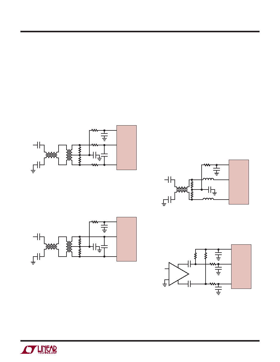
Figure 5. Recommended Front-End Circuit for Input
Frequencies from 150MHz to 250MHz
Figure 6. Recommended Front-End Circuit for Input
Frequencies Above 250MHz
Amplifier Circuits
Figure 7 shows the analog input being driven by a high
speed differential amplifier. The output of the amplifier is
AC-coupled to the A/D so the amplifier’s output common
mode voltage can be optimally set to minimize distortion.
At very high frequencies an RF gain block will often have
lower distortion than a differential amplifier. If the gain
block is single-ended, then a transformer circuit (Figure 4
to Figure 6) should convert the signal to differential before
driving the A/D.
Figure 4. Recommended Front-End Circuit for Input
Frequencies from 5MHz to 150MHz
Reference
The LTC2145-14/LTC2144-14/LTC2143-14 has an internal
1.25V voltage reference. For a 2V input range using the
internal reference, connect SENSE to VDD. For a 1V input
range using the internal reference, connect SENSE to
ground. For a 2V input range with an external reference,
apply a 1.25V reference voltage to SENSE (Figure 9).
The input range can be adjusted by applying a voltage to
SENSE that is between 0.625V and 1.30V. The input range
will then be 1.6 VSENSE.
The VREF, REFH and REFL pins should be bypassed as
shown in Figure 8. A low inductance 2.2μF interdigitated
capacitor is recommended for the bypass between REFH
and REFL. This type of capacitor is available at a low cost
from multiple suppliers.
25Ω
12Ω
25Ω
50Ω
0.1μF
AIN
+
AIN
–
8.2pF
0.1μF
VCM
ANALOG
INPUT
0.1μF
T1
T2
T1: MA/COM MABA-007159-000000
T2: COILCRAFT WBC1-1TL
RESISTORS, CAPACITORS ARE 0402 PACKAGE SIZE
21454314 F04
LTC2145-14
25Ω
50Ω
0.1μF
AIN
+
AIN
–
1.8pF
0.1μF
VCM
ANALOG
INPUT
0.1μF
T1
T2
T1: MA/COM MABA-007159-000000
T2: COILCRAFT WBC1-1TL
RESISTORS, CAPACITORS ARE 0402 PACKAGE SIZE
21454314 F05
LTC2145-14
25Ω
50Ω
0.1μF
4.7nH
AIN
+
AIN
–
0.1μF
VCM
ANALOG
INPUT
T1: MA/COM ETC1-1-13
RESISTORS, CAPACITORS
ARE 0402 PACKAGE SIZE
21454314 F06
LTC2145-14
T1
0.1μF
25Ω
200Ω
0.1μF
AIN
+
AIN
–
0.1μF
12pF
VCM
LTC2145-14
21454314 F07
–
+
ANALOG
INPUT
HIGH SPEED
DIFFERENTIAL
AMPLIFIER
0.1μF
Figure 7. Front-End Circuit Using a High Speed
Differential Amplifier
相关PDF资料 |
PDF描述 |
|---|---|
| LTC1347CSW | IC TXRX 5V RS232 LOW PWR 28-SOIC |
| LTC1347CNW | IC TXRX 5V RS232 LOW PWR 28-DIP |
| VE-26D-MX-F1 | CONVERTER MOD DC/DC 85V 75W |
| AD9627ABCPZ-105 | IC ADC 12BIT 105MSPS 64LFCSP |
| SP233ECT-L | IC DVR/RCVR RS232 5V SGL 20WSOIC |
相关代理商/技术参数 |
参数描述 |
|---|---|
| LTC2144-12 | 制造商:LINER 制造商全称:Linear Technology 功能描述:12-Bit, 125Msps/105Msps/ 80Msps Low Power Dual ADCs |
| LTC2144-14 | 制造商:LINER 制造商全称:Linear Technology 功能描述:12-Bit, 125Msps/105Msps/ 80Msps Low Power Dual ADCs |
| LTC2144CUP-12#PBF | 功能描述:IC ADC DUAL 12BIT 105MSPS 64-QFN RoHS:是 类别:集成电路 (IC) >> 数据采集 - 模数转换器 系列:- 标准包装:1 系列:- 位数:14 采样率(每秒):83k 数据接口:串行,并联 转换器数目:1 功率耗散(最大):95mW 电压电源:双 ± 工作温度:0°C ~ 70°C 安装类型:通孔 封装/外壳:28-DIP(0.600",15.24mm) 供应商设备封装:28-PDIP 包装:管件 输入数目和类型:1 个单端,双极 |
| LTC2144CUP-12#TRPBF | 功能描述:IC ADC DUAL 12BIT 105MSPS 64-QFN RoHS:是 类别:集成电路 (IC) >> 数据采集 - 模数转换器 系列:- 标准包装:1 系列:- 位数:14 采样率(每秒):83k 数据接口:串行,并联 转换器数目:1 功率耗散(最大):95mW 电压电源:双 ± 工作温度:0°C ~ 70°C 安装类型:通孔 封装/外壳:28-DIP(0.600",15.24mm) 供应商设备封装:28-PDIP 包装:管件 输入数目和类型:1 个单端,双极 |
| LTC2144CUP-14#PBF | 功能描述:IC ADC DUAL 14BIT 105MSPS 64-QFN RoHS:是 类别:集成电路 (IC) >> 数据采集 - 模数转换器 系列:- 其它有关文件:TSA1204 View All Specifications 标准包装:1 系列:- 位数:12 采样率(每秒):20M 数据接口:并联 转换器数目:2 功率耗散(最大):155mW 电压电源:模拟和数字 工作温度:-40°C ~ 85°C 安装类型:表面贴装 封装/外壳:48-TQFP 供应商设备封装:48-TQFP(7x7) 包装:Digi-Reel® 输入数目和类型:4 个单端,单极;2 个差分,单极 产品目录页面:1156 (CN2011-ZH PDF) 其它名称:497-5435-6 |
发布紧急采购,3分钟左右您将得到回复。