- 您现在的位置:买卖IC网 > PDF目录10031 > LTC2153IUJ-14#TRPBF (Linear Technology)IC ADC 14BIT DUAL 310MSPS 40QFN PDF资料下载
参数资料
| 型号: | LTC2153IUJ-14#TRPBF |
| 厂商: | Linear Technology |
| 文件页数: | 24/24页 |
| 文件大小: | 0K |
| 描述: | IC ADC 14BIT DUAL 310MSPS 40QFN |
| 标准包装: | 2,000 |
| 位数: | 14 |
| 采样率(每秒): | 310M |
| 数据接口: | 并联,串行,SPI |
| 转换器数目: | 1 |
| 功率耗散(最大): | 479mW |
| 电压电源: | 模拟和数字 |
| 工作温度: | -40°C ~ 85°C |
| 安装类型: | 表面贴装 |
| 封装/外壳: | 40-WFQFN 裸露焊盘 |
| 供应商设备封装: | 40-QFN(6x6) |
| 包装: | 带卷 (TR) |
| 输入数目和类型: | 1 个差分 |
| 配用: | DC1371A-ND - BOARD USB DATA ACQUISITION HS |
9
215314f
LTC2153-14
pin FuncTions
SCK (Pin 38): Serial Interface Clock Input. In serial
programming mode, (PAR/SER = 0V), SCK is the serial
interfaceclockinput.Inparallelprogrammingmode(PAR/
SER = VDD), SCK controls the sleep mode (see Table 2).
CS (Pin 39): Serial Interface Chip Select Input. In serial
programming mode, (PAR/SER = 0V), CS is the serial in-
terface chip select input. When CS is low, SCK is enabled
for shifting data on SDI into the mode control registers. In
parallelprogrammingmode(PAR/SER=VDD),CScontrols
the clock duty cycle stabilizer (see Table 2).
PAR/SER (Pin 40): Programming Mode Selection Pin.
Connect to ground to enable the serial programming
mode. CS, SCK, SDI and SDO become a serial interface
that control the A/D operating modes. Connect to VDD to
enabletheparallelprogrammingmodewhereCS,SCKand
SDI become parallel logic inputs that control a reduced
set of the A/D operating modes. PAR/SER should be con-
nected directly to ground or the VDD of the part and not
be driven by a logic signal.
LVDS Outputs (DDR LVDS)
The following pins are differential LVDS outputs. The
output current level is programmable. There is an optional
internal 100 termination resistor between the pins of
each LVDS output pair.
D0_1–/D0_1+ to D12_13–/D12_13+ (Pins 16/17, 18/19,
22/23, 24/25, 28/29, 31/32, 33/34): Double-Data Rate
Digital Outputs. Two data bits are multiplexed onto each
differential output pair. The even data bits (D0, D2, D4,
D6, D8, D10, D12) appear when CLKOUT+ is low. The odd
data bits (D1, D3, D5, D7, D9, D11, D13) appear when
CLKOUT+ is high.
CLKOUT–, CLKOUT+ (Pins 26, 27): Data Output Clock.
The digital outputs normally transition at the same time
as the falling and rising edges of CLKOUT+. The phase of
CLKOUT+ can also be delayed relative to the digital outputs
by programming the mode control registers.
OF–, OF+ (Pins 14, 15): Over/Underflow Digital Output.
OF+ is high when an overflow or underflow has occurred.
This underflow is valid only when CLKOUT+ is low. In the
second half clock cycle, the overflow is set to 0.
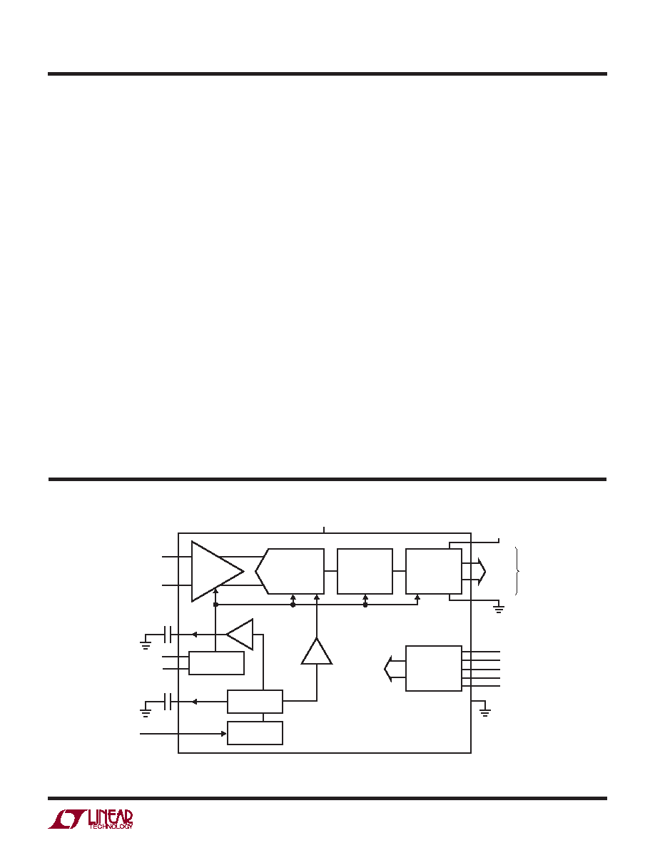
FuncTional block DiagraM
Figure 1. Functional Block Diagram
S/H
VCM
BUFFER
GND
VCM
0.1F
CORRECTION
LOGIC
OUTPUT
DRIVERS
14-BIT
PIPELINED
ADC
CLOCK/DUTY
CYCLE CONTROL
1.25V
REFERENCE
RANGE
SELECT
CLOCK
ANALOG
INPUT
215314 F01
DDR
LVDS
VDD
OVDD
OGND
CS
SPI
VREF
2.2F
GND
SENSE
SCK
SDI
SDO
PAR/SER
D12_13
D0_1
相关PDF资料 |
PDF描述 |
|---|---|
| MS3112E24-61PX | CONN RCPT 61POS BOX MNT W/PINS |
| AD679AJ | IC ADC 14BIT SAMPLING 44-JLCC |
| VI-26M-MX-F3 | CONVERTER MOD DC/DC 10V 75W |
| MS3112E24-61P | CONN RCPT 61POS BOX MNT W/PINS |
| IDT72V3612L15PF8 | IC FIFO 64X36X2 15NS 120QFP |
相关代理商/技术参数 |
参数描述 |
|---|---|
| LTC2155-12 | 制造商:LINER 制造商全称:Linear Technology 功能描述:Dual 14-Bit 250Msps |
| LTC2155-14 | 制造商:LINER 制造商全称:Linear Technology 功能描述:300MHz Digital Predistortion Receiver |
| LTC2155CUP-12 | 制造商:Linear Technology 功能描述:ADC DUAL 12BIT 170M 64QFN 制造商:Linear Technology 功能描述:ADC, DUAL, 12BIT, 170M, 64QFN |
| LTC2155CUP-12#PBF | 功能描述:IC ADC DUAL 12BIT 170M 64-QFN RoHS:是 类别:集成电路 (IC) >> 数据采集 - 模数转换器 系列:- 其它有关文件:TSA1204 View All Specifications 标准包装:1 系列:- 位数:12 采样率(每秒):20M 数据接口:并联 转换器数目:2 功率耗散(最大):155mW 电压电源:模拟和数字 工作温度:-40°C ~ 85°C 安装类型:表面贴装 封装/外壳:48-TQFP 供应商设备封装:48-TQFP(7x7) 包装:Digi-Reel® 输入数目和类型:4 个单端,单极;2 个差分,单极 产品目录页面:1156 (CN2011-ZH PDF) 其它名称:497-5435-6 |
| LTC2155CUP-12#TRPBF | 功能描述:IC ADC DUAL 12BIT 170M 64-QFN RoHS:是 类别:集成电路 (IC) >> 数据采集 - 模数转换器 系列:- 标准包装:1 系列:- 位数:14 采样率(每秒):83k 数据接口:串行,并联 转换器数目:1 功率耗散(最大):95mW 电压电源:双 ± 工作温度:0°C ~ 70°C 安装类型:通孔 封装/外壳:28-DIP(0.600",15.24mm) 供应商设备封装:28-PDIP 包装:管件 输入数目和类型:1 个单端,双极 |
发布紧急采购,3分钟左右您将得到回复。