- 您现在的位置:买卖IC网 > PDF目录10031 > AD679AJ (Analog Devices Inc)IC ADC 14BIT SAMPLING 44-JLCC PDF资料下载
参数资料
| 型号: | AD679AJ |
| 厂商: | Analog Devices Inc |
| 文件页数: | 1/16页 |
| 文件大小: | 0K |
| 描述: | IC ADC 14BIT SAMPLING 44-JLCC |
| 标准包装: | 1 |
| 位数: | 14 |
| 采样率(每秒): | 128k |
| 数据接口: | 并联 |
| 转换器数目: | 2 |
| 功率耗散(最大): | 745mW |
| 电压电源: | 模拟和数字,双 ± |
| 工作温度: | -40°C ~ 85°C |
| 安装类型: | 表面贴装 |
| 封装/外壳: | 44-LCC(J 形引线) |
| 供应商设备封装: | 44-JLCC(16.39x16.39) |
| 包装: | 管件 |
| 输入数目和类型: | 1 个单端,单极;1 个单端,双极 |
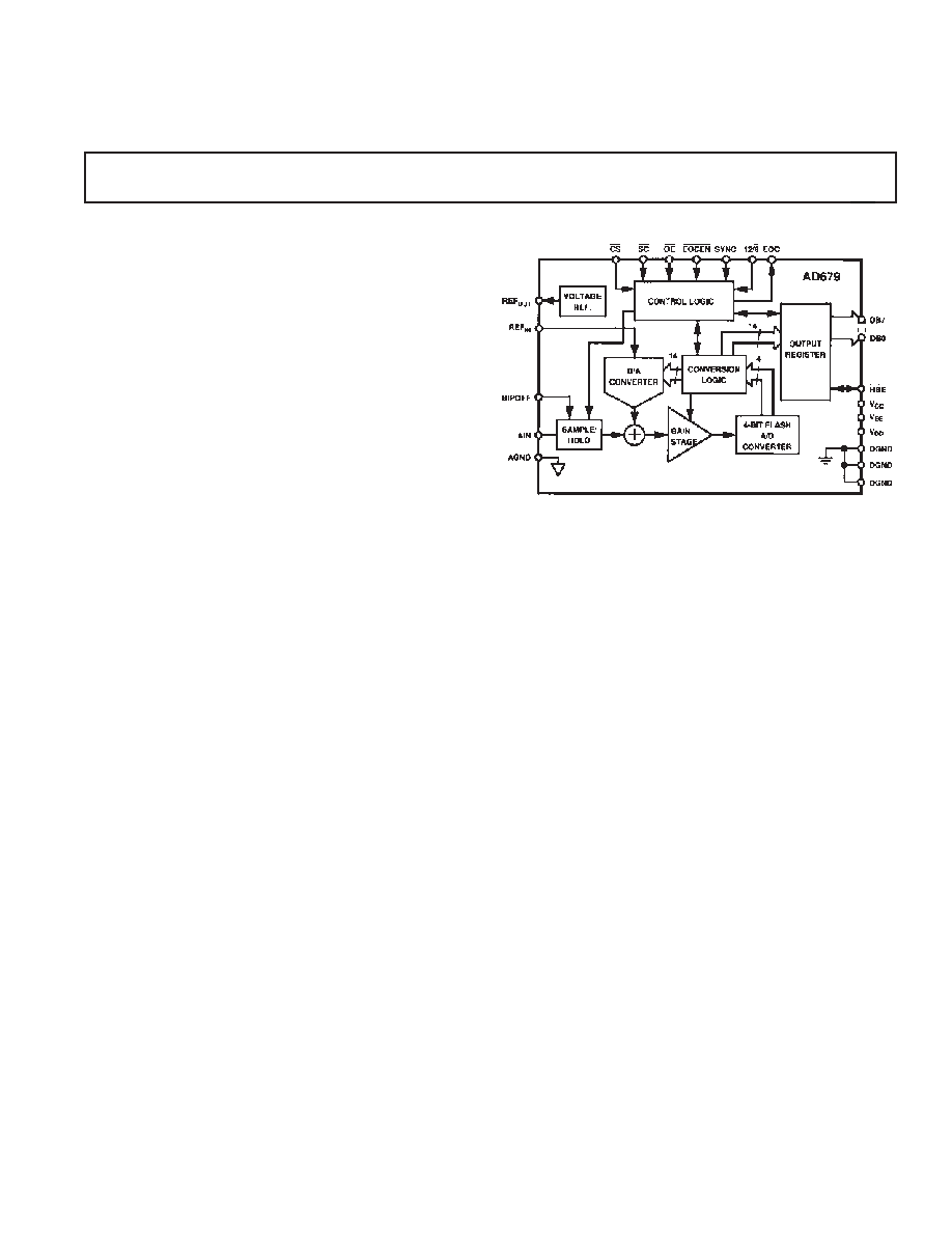
FUNCTIONAL BLOCK DIAGRAM
REV. D
a
14-Bit 128 kSPS
Complete Sampling ADC
AD679
FEATURES
AC and DC Characterized and Specified
(K, B, T Grades)
128k Conversions per Second
1 MHz Full Power Bandwidth
500 kHz Full Linear Bandwidth
78 dB S/N+D (K, B, T Grades)
Twos Complement Data Format (Bipolar Mode)
Straight Binary Data Format (Unipolar Mode)
10 M
Input Impedance
8-Bit Bus Interface
On-Board Reference and Clock
10 V Unipolar or Bipolar Input Range
Pin Compatible with AD678 12-Bit, 200 kSPS ADC
MIL-STD-883 Compliant Versions Available
PRODUCT HIGHLIGHTS
1. COMPLETE INTEGRATION: The AD679 minimizes
external component requirements by combining a high
speed sample-and-hold amplifier (SHA), ADC, 5 V refer-
ence, clock, and digital interface on a single chip. This
provides a fully specified sampling A/D function unattain-
able with discrete designs.
2. SPECIFICATIONS: The AD679K, B, and T grades provide
fully specified and tested ac and dc parameters. The AD679J,
A, and S grades are specified and tested for ac parameters; dc
accuracy specifications are shown as typicals. DC specifica-
tions (such as INL, gain, and offset) are important in control
and measurement applications. AC specifications (such as
S/N+D ratio, THD, and IMD) are of value in signal process-
ing applications.
3. EASE OF USE: The pinout is designed for easy board layout,
and the two-read output provides compatibility with 8-bit
buses. Factory trimming eliminates the need for calibration
modes or external trimming to achieve rated performance.
4. RELIABILITY: The AD679 utilizes Analog Devices’ mono-
lithic BiMOS technology. This ensures long-term reliability
compared to multichip and hybrid designs.
5. UPGRADE PATH: The AD679 provides the same pinout as
the 12-bit, 200 kSPS AD678 ADC.
6. The AD679 is available in versions compliant with MIL-
STD-883. Refer to the Analog Devices Military Products
Databook or current AD679/883B data sheet for detailed
specifications.
GENERAL DESCRIPTION
The AD679 is a complete, multipurpose 14-bit monolithic
analog-to-digital converter, consisting of a sample-and-hold am-
plifier (SHA), a microprocessor-compatible bus interface, a volt-
age reference, and clock generation circuitry.
The AD679 is specified for ac (or dynamic) parameters such as
S/N+D ratio, THD, and IMD, which are important in signal
processing applications. In addition, the AD679K, B, and T
grades are fully specified for dc parameters that are important in
measurement applications.
The 14 data bits are accessed in two read operations (8 + 6),
with left justification. Data format is straight binary for unipolar
mode and twos complement binary for bipolar mode. The input
has a full-scale range of 10 V with a full power bandwidth of
1 MHz and a full linear bandwidth of 500 kHz. High input
impedance (10 M
) allows direct connection to unbuffered
sources without signal degradation. Conversions can be initiated
either under microprocessor control or by an external clock
asynchronous to the system clock.
This product is fabricated on Analog Devices’ BiMOS process,
combining low power CMOS logic with high precision, low
noise bipolar circuits; laser-trimmed thin-film resistors provide
high accuracy. The converter utilizes a recursive subranging
algorithm that includes error correction and flash converter
circuitry to achieve high speed and resolution.
The AD679 operates from +5 V and
±12 V supplies and dissipates
560 mW (typ). The part is available in 28-lead plastic DIP,
ceramic DIP, and 44 J-leaded ceramic surface-mount packages.
Information furnished by Analog Devices is believed to be accurate and
reliable. However, no responsibility is assumed by Analog Devices for its
use, nor for any infringements of patents or other rights of third parties that
may result from its use. No license is granted by implication or otherwise
under any patent or patent rights of Analog Devices. Trademarks and
registered trademarks are the property of their respective owners.
One Technology Way, P.O. Box 9106, Norwood, MA 02062-9106, U.S.A.
Tel: 781/329-4700
Fax: 781/326-8703
2004 Analog Devices, Inc. All rights reserved.
相关PDF资料 |
PDF描述 |
|---|---|
| VI-26M-MX-F3 | CONVERTER MOD DC/DC 10V 75W |
| MS3112E24-61P | CONN RCPT 61POS BOX MNT W/PINS |
| IDT72V3612L15PF8 | IC FIFO 64X36X2 15NS 120QFP |
| AD678BD | IC ADC 12BIT SAMPLING 28-CDIP |
| AD1555BPZRL | IC ADC PGA 24BIT LN 28-PLCC |
相关代理商/技术参数 |
参数描述 |
|---|---|
| AD679AJZ | 制造商:Analog Devices 功能描述:ADC SGL FLASH 128KSPS 14BIT PARALLEL 44PIN JLCC - Rail/Tube |
| AD679BD | 功能描述:IC ADC 14BIT SAMPLING 28-CDIP RoHS:否 类别:集成电路 (IC) >> 数据采集 - 模数转换器 系列:- 产品培训模块:Lead (SnPb) Finish for COTS Obsolescence Mitigation Program 标准包装:250 系列:- 位数:12 采样率(每秒):1.8M 数据接口:并联 转换器数目:1 功率耗散(最大):1.82W 电压电源:模拟和数字 工作温度:-40°C ~ 85°C 安装类型:表面贴装 封装/外壳:48-LQFP 供应商设备封装:48-LQFP(7x7) 包装:管件 输入数目和类型:2 个单端,单极 |
| AD679BJ | 功能描述:IC ADC 14BIT SAMPLING 44-JLCC RoHS:否 类别:集成电路 (IC) >> 数据采集 - 模数转换器 系列:- 产品培训模块:Lead (SnPb) Finish for COTS Obsolescence Mitigation Program 标准包装:250 系列:- 位数:12 采样率(每秒):1.8M 数据接口:并联 转换器数目:1 功率耗散(最大):1.82W 电压电源:模拟和数字 工作温度:-40°C ~ 85°C 安装类型:表面贴装 封装/外壳:48-LQFP 供应商设备封装:48-LQFP(7x7) 包装:管件 输入数目和类型:2 个单端,单极 |
| AD679JD | 功能描述:IC ADC 14BIT SAMPLING 28-CDIP RoHS:否 类别:集成电路 (IC) >> 数据采集 - 模数转换器 系列:- 产品培训模块:Lead (SnPb) Finish for COTS Obsolescence Mitigation Program 标准包装:250 系列:- 位数:12 采样率(每秒):1.8M 数据接口:并联 转换器数目:1 功率耗散(最大):1.82W 电压电源:模拟和数字 工作温度:-40°C ~ 85°C 安装类型:表面贴装 封装/外壳:48-LQFP 供应商设备封装:48-LQFP(7x7) 包装:管件 输入数目和类型:2 个单端,单极 |
| AD679JN | 功能描述:IC ADC 14BIT 128KSPS 28-DIP RoHS:否 类别:集成电路 (IC) >> 数据采集 - 模数转换器 系列:- 标准包装:1 系列:- 位数:14 采样率(每秒):83k 数据接口:串行,并联 转换器数目:1 功率耗散(最大):95mW 电压电源:双 ± 工作温度:0°C ~ 70°C 安装类型:通孔 封装/外壳:28-DIP(0.600",15.24mm) 供应商设备封装:28-PDIP 包装:管件 输入数目和类型:1 个单端,双极 |
发布紧急采购,3分钟左右您将得到回复。