- 您现在的位置:买卖IC网 > PDF目录10031 > AD679AJ (Analog Devices Inc)IC ADC 14BIT SAMPLING 44-JLCC PDF资料下载
参数资料
| 型号: | AD679AJ |
| 厂商: | Analog Devices Inc |
| 文件页数: | 2/16页 |
| 文件大小: | 0K |
| 描述: | IC ADC 14BIT SAMPLING 44-JLCC |
| 标准包装: | 1 |
| 位数: | 14 |
| 采样率(每秒): | 128k |
| 数据接口: | 并联 |
| 转换器数目: | 2 |
| 功率耗散(最大): | 745mW |
| 电压电源: | 模拟和数字,双 ± |
| 工作温度: | -40°C ~ 85°C |
| 安装类型: | 表面贴装 |
| 封装/外壳: | 44-LCC(J 形引线) |
| 供应商设备封装: | 44-JLCC(16.39x16.39) |
| 包装: | 管件 |
| 输入数目和类型: | 1 个单端,单极;1 个单端,双极 |
AD679
REV. D
–10–
INPUT CONNECTIONS AND CALIBRATION
The high (10 M
) input impedance of the AD679 eases the
task of interfacing to high source impedances or multiplexer
channel-to-channel mismatches of up to 300
. The 10 V p-p
full-scale input range accepts the majority of signal voltages
without the need for voltage divider networks that could deterio-
rate the accuracy of the ADC.
The AD679 is factory trimmed to minimize offset, gain, and
linearity errors. In unipolar mode, the only external component
that is required is a 50
1% resistor. Two resistors are required
in bipolar mode. If offset and gain are not critical (as in some ac
applications), even these components can be eliminated.
In some applications, offset and gain errors need to be trimmed
out completely. The following sections describe the correct pro-
cedure for these various situations.
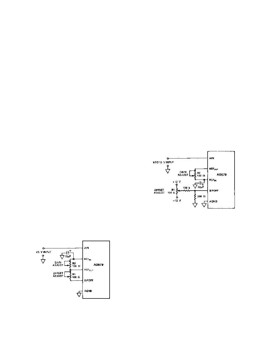
Bipolar Range Inputs
The connections for the bipolar mode are shown in Figure 5. In
this mode, data output coding is twos complement binary. This
circuit allows approximately
25 mV of offset trim range ( 40
LSB) and
0.5% of gain trim range ( 80 LSB).
Either or both of the trim pots can be replaced with 50
1%
fixed resistors if the AD679 accuracy limits are sufficient for
application. If the pins are shorted together, the additional offset
and gain error is approximately 80 LSB.
To trim bipolar zero to its nominal value, apply a signal 1/2 LSB
below midrange (–0.305 mV for a
5 V range) and adjust R1
until the major carry transition is located (11 1111 1111 1111 to
00 0000 0000 0000). To trim the gain, apply a signal 1 1/2 LSB
below full scale (+4.9991 V for a
5 V range) and adjust R2 to
give the last positive transition (01 1111 1111 1110 to 01 1111
1111 1111). These trims are interactive so several iterations may
be necessary for convergence.
A single pass calibration can be done by substituting a bipolar
offset trim (error at minus full scale) for the bipolar zero trim
(error at midscale) using the same circuit. First, apply a
signal 1/2 LSB above minus full scale (–4.9997 V for a
5 V
range) and adjust R1 until the minus full-scale transition is lo-
cated (10 0000 0000 0000 to 10 000 000 0001). Then perform
the gain error trim as outlined above.
Figure 5. Bipolar Input Connections with Gain and
Offset Trims
Unipolar Range Inputs
Offset and gain errors can be trimmed out by using the configu-
ration shown in Figure 6. This circuit allows approximately
25 mV of offset trim range ( 40 LSB) and
0.5% of gain
trim range ( 80 LSB).
The nominal offset is 1/2 LSB so that the analog range that cor-
responds to each code is centered in the middle of that code
(halfway between the transitions to the codes above and below
it). Thus the first transition (from 00 0000 0000 0000 to 00
0000 0000 0001) should nominally occur for an input level of
+1/2 LSB (0.305 mV above ground for a 10 V range). To trim
unipolar zero to this nominal value, apply a 0.305 mV signal to
AIN and adjust R1 until the first transition is located.
The gain trim is done by adjusting R2. If the nominal value is
required, apply a signal 1 1/2 LSB below full scale (9.9997 V for
a 10 V range) and adjust R2 until the last transition is located
(11 1111 1111 1110 to 11 1111 1111 1111).
If offset adjustment is not required, BIPOFF should be con-
nected directly to AGND. If gain adjustment is not required, R2
should be replaced with a fixed 50
1% metal film resistor. If
REFOUT is connected directly to REFIN, the additional gain
error is approximately 1%.
Figure 6. Unipolar Input Connections with Gain and
Offset Trims
REFERENCE DECOUPLING
It is recommended that a 10
F tantalum capacitor be con-
nected between REFIN (Pin 9) and ground. This has the effect
of improving the S/N+D ratio through filtering possible broad-
band noise contributions from the voltage reference.
BOARD LAYOUT
Designing with high resolution data converters requires careful
attention to board layout. Trace impedance is a significant issue.
A 1.22 mA current through a 0.5
trace will develop a voltage
drop of 0.6 mV, which is 1 LSB at the 14-bit level for a 10 V
full-scale span. In addition to ground drops, inductive and
capacitive coupling need to be considered, especially when high
accuracy analog signals share the same board with digital signals.
Finally, power supplies need to be decoupled in order to filter
out ac noise.
Analog and digital signals should not share a common path.
Each signal should have an appropriate analog or digital return
routed close to it. Using this approach, signal loops enclose a
small area, minimizing the inductive coupling of noise. Wide PC
tracks, large gauge wire, and ground planes are highly recom-
mended to provide low impedance signal paths. Separate analog
相关PDF资料 |
PDF描述 |
|---|---|
| VI-26M-MX-F3 | CONVERTER MOD DC/DC 10V 75W |
| MS3112E24-61P | CONN RCPT 61POS BOX MNT W/PINS |
| IDT72V3612L15PF8 | IC FIFO 64X36X2 15NS 120QFP |
| AD678BD | IC ADC 12BIT SAMPLING 28-CDIP |
| AD1555BPZRL | IC ADC PGA 24BIT LN 28-PLCC |
相关代理商/技术参数 |
参数描述 |
|---|---|
| AD679AJZ | 制造商:Analog Devices 功能描述:ADC SGL FLASH 128KSPS 14BIT PARALLEL 44PIN JLCC - Rail/Tube |
| AD679BD | 功能描述:IC ADC 14BIT SAMPLING 28-CDIP RoHS:否 类别:集成电路 (IC) >> 数据采集 - 模数转换器 系列:- 产品培训模块:Lead (SnPb) Finish for COTS Obsolescence Mitigation Program 标准包装:250 系列:- 位数:12 采样率(每秒):1.8M 数据接口:并联 转换器数目:1 功率耗散(最大):1.82W 电压电源:模拟和数字 工作温度:-40°C ~ 85°C 安装类型:表面贴装 封装/外壳:48-LQFP 供应商设备封装:48-LQFP(7x7) 包装:管件 输入数目和类型:2 个单端,单极 |
| AD679BJ | 功能描述:IC ADC 14BIT SAMPLING 44-JLCC RoHS:否 类别:集成电路 (IC) >> 数据采集 - 模数转换器 系列:- 产品培训模块:Lead (SnPb) Finish for COTS Obsolescence Mitigation Program 标准包装:250 系列:- 位数:12 采样率(每秒):1.8M 数据接口:并联 转换器数目:1 功率耗散(最大):1.82W 电压电源:模拟和数字 工作温度:-40°C ~ 85°C 安装类型:表面贴装 封装/外壳:48-LQFP 供应商设备封装:48-LQFP(7x7) 包装:管件 输入数目和类型:2 个单端,单极 |
| AD679JD | 功能描述:IC ADC 14BIT SAMPLING 28-CDIP RoHS:否 类别:集成电路 (IC) >> 数据采集 - 模数转换器 系列:- 产品培训模块:Lead (SnPb) Finish for COTS Obsolescence Mitigation Program 标准包装:250 系列:- 位数:12 采样率(每秒):1.8M 数据接口:并联 转换器数目:1 功率耗散(最大):1.82W 电压电源:模拟和数字 工作温度:-40°C ~ 85°C 安装类型:表面贴装 封装/外壳:48-LQFP 供应商设备封装:48-LQFP(7x7) 包装:管件 输入数目和类型:2 个单端,单极 |
| AD679JN | 功能描述:IC ADC 14BIT 128KSPS 28-DIP RoHS:否 类别:集成电路 (IC) >> 数据采集 - 模数转换器 系列:- 标准包装:1 系列:- 位数:14 采样率(每秒):83k 数据接口:串行,并联 转换器数目:1 功率耗散(最大):95mW 电压电源:双 ± 工作温度:0°C ~ 70°C 安装类型:通孔 封装/外壳:28-DIP(0.600",15.24mm) 供应商设备封装:28-PDIP 包装:管件 输入数目和类型:1 个单端,双极 |
发布紧急采购,3分钟左右您将得到回复。