- 您现在的位置:买卖IC网 > PDF目录10031 > AD679AJ (Analog Devices Inc)IC ADC 14BIT SAMPLING 44-JLCC PDF资料下载
参数资料
| 型号: | AD679AJ |
| 厂商: | Analog Devices Inc |
| 文件页数: | 16/16页 |
| 文件大小: | 0K |
| 描述: | IC ADC 14BIT SAMPLING 44-JLCC |
| 标准包装: | 1 |
| 位数: | 14 |
| 采样率(每秒): | 128k |
| 数据接口: | 并联 |
| 转换器数目: | 2 |
| 功率耗散(最大): | 745mW |
| 电压电源: | 模拟和数字,双 ± |
| 工作温度: | -40°C ~ 85°C |
| 安装类型: | 表面贴装 |
| 封装/外壳: | 44-LCC(J 形引线) |
| 供应商设备封装: | 44-JLCC(16.39x16.39) |
| 包装: | 管件 |
| 输入数目和类型: | 1 个单端,单极;1 个单端,双极 |
AD679
REV. D
–9–
CONVERSION CONTROL
In synchronous mode (SYNC = HIGH), both chip select (
CS)
and start convert (
SC) must be brought LOW to start a conver-
sion.
CS should be LOW t
SC before SC is brought LOW. In
asynchronous mode (SYNC = LOW), a conversion is started by
bringing
SC low, regardless of the state of CS.
Before a conversion is started, end-of-convert (EOC) is HIGH
and the sample-and-hold is in track mode. After a conversion is
started, the sample-and-hold goes into hold mode and EOC
goes LOW, signifying that a conversion is in progress. During
the conversion, the sample-and-hold will go back into track
mode and start acquiring the next sample.
In track mode, the sample-and-hold will settle to
0.003%
(14 bits) in 1.5
s maximum. The acquisition time does not
affect the throughput rate as the AD679 goes back into track
mode more than 2
s before the next conversion. In multichan-
nel systems, the input channel can be switched as soon as EOC
goes LOW.
Bringing
OE LOW t
OE after CS goes LOW makes the output
register contents available on the output data bits (DB7–DB0).
A period of time, tCD, is required after OE is brought HIGH
before the next SC instruction is issued.
If
SC is held LOW, conversion accuracy may deteriorate. For
this reason,
SC should not be held low in an attempt to operate
in a continuously converting mode.
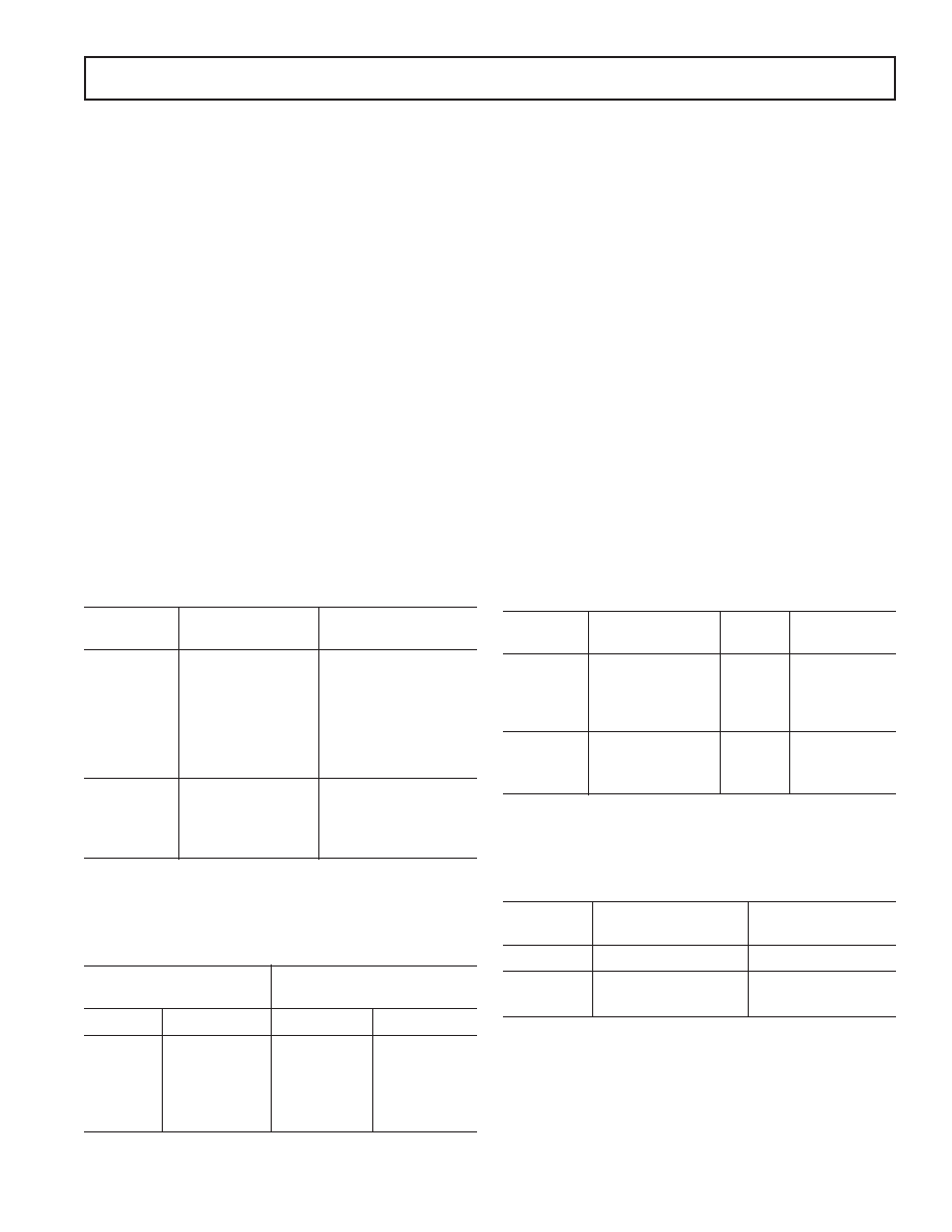
Table I. Start Conversion Truth Table
Inputs
SYNC
CS
SC
Status
Synchronous
1
X
No Conversion
Mode
1
0
f
Start Conversion
1
f
0
Start Conversion
(Not Recommended)
10
0Continuous Conversion
(Not Recommended)
Asynchronous
0
X
1
No Conversion
Mode
0
X
f
Start Conversion
0X
0Continuous Conversion
(Not Recommended)
1= HIGH voltage level.
0= LOW voltage level.
X= Don’t care.
f = HIGH to LOW transition. Must stay low for t = tCP.
Table II. 14-Bit Mode Coding Format (1 LSB = 0.61 mV)
Unipolar Coding
Bipolar Coding
(Straight Binary)
(Twos Complement)
VIN*
Output Code
VIN* (V)
Output Code
0.00000 V
000 . . . 0
–5.00000
100 . . . 0
5.00000 V
100 . . . 0
–0.00061
111 . . . 1
9.99939 V
111 . . . 1
0.00000
000 . . . 0
+2.50000
010 . . . 0
+4.99939
011 . . . 1
*Code center.
END-OF-CONVERT
In asynchronous mode, end-of-convert (EOC) is an open-drain
output (requiring a minimum 3 k
pull-up resistor) enabled by
end-of-convert enable (
EOCEN). In synchronous mode, EOC
is a three-state output that is enabled by
EOCEN and CS. See
Table III. Access (tBA) and float (tFD) timing specifications do
not apply in asynchronous mode where they are a function of
the time constant formed by the external load capacitance and
the pull-up resistor.
OUTPUT ENABLE OPERATION
The data bits (DB7–DB0) are three-state outputs that are enabled
by chip select (
CS) and output enable (OE). CS should be
LOW tOE before OE is brought LOW.
When EOC goes HIGH, the conversion is completed and the
output data may be read. The output is read in two steps as a
16-bit word, with the high byte read first, followed by the low
byte. High byte enable (
HBE) controls the output sequence.
The 14-bit result is left justified within the 16-bit field.
In unipolar mode (BIPOFF tied to AGND), the output coding
is straight binary. In bipolar mode (BIPOFF tied to REFOUT),
output coding is twos complement binary.
POWER-UP
The AD679 typically requires 10
s after power-up to reset
internal logic.
Table III. Conversion Status Truth Table
Inputs
Output
SYNC
CS EOCEN EOC
Status
Synchronous
1
0
Converting
Mode
1
0
1
Not Converting
11
XHigh Z
Either
1X
1High Z
Either
Asynchronous
0X
00
Converting
Mode
*
0X
0High Z
Not Converting
0X
1High Z
Either
1 = HIGH voltage level.
0 = LOW voltage level.
X = Don’t care.
*EOC requires a pull-up resistor in asynchronous mode.
Table IV. Output Enable Truth Table
Inputs
Outputs
HBE
(
CS U OE)
DB7 . . . DB0
X1
← High Z →
Unipolar or
0
a b c d e f g h
Bipolar
1
0
i j
k l m n 0 0
1= HIGH voltage level.
a = MSB.
0= LOW voltage level.
n = LSB.
X= Don’t care.
U = Logical OR.
Data coding is binary for unipolar mode and twos complement binary for
bipolar mode.
相关PDF资料 |
PDF描述 |
|---|---|
| VI-26M-MX-F3 | CONVERTER MOD DC/DC 10V 75W |
| MS3112E24-61P | CONN RCPT 61POS BOX MNT W/PINS |
| IDT72V3612L15PF8 | IC FIFO 64X36X2 15NS 120QFP |
| AD678BD | IC ADC 12BIT SAMPLING 28-CDIP |
| AD1555BPZRL | IC ADC PGA 24BIT LN 28-PLCC |
相关代理商/技术参数 |
参数描述 |
|---|---|
| AD679AJZ | 制造商:Analog Devices 功能描述:ADC SGL FLASH 128KSPS 14BIT PARALLEL 44PIN JLCC - Rail/Tube |
| AD679BD | 功能描述:IC ADC 14BIT SAMPLING 28-CDIP RoHS:否 类别:集成电路 (IC) >> 数据采集 - 模数转换器 系列:- 产品培训模块:Lead (SnPb) Finish for COTS Obsolescence Mitigation Program 标准包装:250 系列:- 位数:12 采样率(每秒):1.8M 数据接口:并联 转换器数目:1 功率耗散(最大):1.82W 电压电源:模拟和数字 工作温度:-40°C ~ 85°C 安装类型:表面贴装 封装/外壳:48-LQFP 供应商设备封装:48-LQFP(7x7) 包装:管件 输入数目和类型:2 个单端,单极 |
| AD679BJ | 功能描述:IC ADC 14BIT SAMPLING 44-JLCC RoHS:否 类别:集成电路 (IC) >> 数据采集 - 模数转换器 系列:- 产品培训模块:Lead (SnPb) Finish for COTS Obsolescence Mitigation Program 标准包装:250 系列:- 位数:12 采样率(每秒):1.8M 数据接口:并联 转换器数目:1 功率耗散(最大):1.82W 电压电源:模拟和数字 工作温度:-40°C ~ 85°C 安装类型:表面贴装 封装/外壳:48-LQFP 供应商设备封装:48-LQFP(7x7) 包装:管件 输入数目和类型:2 个单端,单极 |
| AD679JD | 功能描述:IC ADC 14BIT SAMPLING 28-CDIP RoHS:否 类别:集成电路 (IC) >> 数据采集 - 模数转换器 系列:- 产品培训模块:Lead (SnPb) Finish for COTS Obsolescence Mitigation Program 标准包装:250 系列:- 位数:12 采样率(每秒):1.8M 数据接口:并联 转换器数目:1 功率耗散(最大):1.82W 电压电源:模拟和数字 工作温度:-40°C ~ 85°C 安装类型:表面贴装 封装/外壳:48-LQFP 供应商设备封装:48-LQFP(7x7) 包装:管件 输入数目和类型:2 个单端,单极 |
| AD679JN | 功能描述:IC ADC 14BIT 128KSPS 28-DIP RoHS:否 类别:集成电路 (IC) >> 数据采集 - 模数转换器 系列:- 标准包装:1 系列:- 位数:14 采样率(每秒):83k 数据接口:串行,并联 转换器数目:1 功率耗散(最大):95mW 电压电源:双 ± 工作温度:0°C ~ 70°C 安装类型:通孔 封装/外壳:28-DIP(0.600",15.24mm) 供应商设备封装:28-PDIP 包装:管件 输入数目和类型:1 个单端,双极 |
发布紧急采购,3分钟左右您将得到回复。