- 您现在的位置:买卖IC网 > PDF目录10652 > LTC2158CUP-14#PBF (Linear Technology)IC ADC DUAL 14BIT 310M 64-QFN PDF资料下载
参数资料
| 型号: | LTC2158CUP-14#PBF |
| 厂商: | Linear Technology |
| 文件页数: | 11/28页 |
| 文件大小: | 0K |
| 描述: | IC ADC DUAL 14BIT 310M 64-QFN |
| 标准包装: | 40 |
| 位数: | 14 |
| 采样率(每秒): | 310M |
| 数据接口: | 并联,串行,SPI |
| 转换器数目: | 2 |
| 功率耗散(最大): | 873mW |
| 电压电源: | 模拟和数字 |
| 工作温度: | 0°C ~ 70°C |
| 安装类型: | 表面贴装 |
| 封装/外壳: | 64-WFQFN 裸露焊盘 |
| 供应商设备封装: | 64-QFN(9x9) |
| 包装: | 管件 |
| 输入数目和类型: | 2 个差分 |
| 配用: | DC1371A-ND - BOARD USB DATA ACQUISITION HS |
第1页第2页第3页第4页第5页第6页第7页第8页第9页第10页当前第11页第12页第13页第14页第15页第16页第17页第18页第19页第20页第21页第22页第23页第24页第25页第26页第27页第28页
19
215814f
LTC2158-14
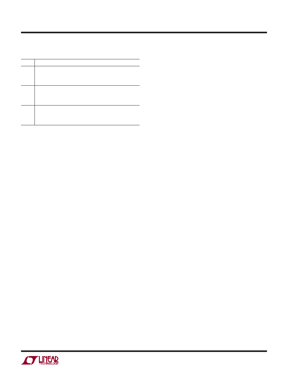
Table 2. Parallel Programming Mode Control Bits (PAR/SER = VDD)
PIN
DESCRIPTION
CS
Clock Duty Cycle Stabilizer Control Bit
0 = Clock Duty Cycle Stabilizer Off
1 = Clock Duty Cycle Stabilizer On
SCK
Power Down Control Bit
0 = Normal Operation
1 = Sleep Mode (entire ADC is powered down)
SDI
LVDS Current Selection Bit
0 = 3.5mA LVDS Current Mode
1 = 1.75mA LVDS Current Mode
Serial Programming Mode
To use the serial programming mode, PAR/SER should be
tied to ground. The CS, SCK, SDI and SDO pins become
a serial interface that program the A/D control registers.
Data is written to a register with a 16-bit serial word. Data
can also be read back from a register to verify its contents.
Serial data transfer starts when CS is taken low. The data
on the SDI pin is latched at the first sixteen rising edges
of SCK. Any SCK rising edges after the first sixteen are
ignored.ThedatatransferendswhenCSistakenhighagain.
The first bit of the 16-bit input word is the R/W bit. The
next seven bits are the address of the register (A6:A0).
The final eight bits are the register data (D7:D0).
If the R/W bit is low, the serial data (D7:D0) will be writ-
ten to the register set by the address bits (A6:A0). If the
R/W bit is high, data in the register set by the address bits
(A6:A0) will be read back on the SDO pin (see the Timing
Diagrams). During a readback command the register is
not updated and data on SDI is ignored.
The SDO pin is an open-drain output that pulls to ground
with a 200 impedance. If register data is read back
through SDO, an external 2k pull-up resistor is required.
If serial data is only written and readback is not needed,
then SDO can be left floating and no pull-up resistor is
needed.Table 3showsamapofthemodecontrolregisters.
Software Reset
If serial programming is used, the mode control registers
shouldbeprogrammedassoonaspossibleafterthepower
supplies turn on and are stable. The first serial command
must be a software reset which will reset all register data
bits to logic 0. To perform a software reset it is neces-
sary to write 1 in register A0 (Bit D7). After the reset is
complete, Bit D7 is automatically set back to zero. This
register is write-only.
GROUNDING AND BYPASSING
The LTC2158-14 requires a printed circuit board with a
clean unbroken ground plane in the first layer beneath the
ADC. A multilayer board with an internal ground plane is
recommended. Layout for the printed circuit board should
ensure that digital and analog signal lines are separated as
much as possible. In particular, care should be taken not
to run any digital track alongside an analog signal track
or underneath the ADC.
High quality ceramic bypass capacitors should be used at
the VDD,OVDD,VCM,VREF pins.Bypasscapacitorsmustbe
located as close to the pins as possible. Size 0402 ceramic
capacitors are recommended. The traces connecting the
pins and bypass capacitors must be kept short and should
be made as wide as possible.
The analog inputs, encode signals, and digital outputs
should not be routed next to each other. Ground fill and
grounded vias should be used as barriers to isolate these
signals from each other.
HEAT TRANSFER
Most of the heat generated by the LTC2158-14 is trans-
ferred from the die through the bottom-side exposed pad
and package leads onto the printed circuit board. For good
electrical and thermal performance, the exposed pad must
be soldered to a large grounded pad on the PC board. This
pad should be connected to the internal ground planes by
an array of vias.
applicaTions inForMaTion
相关PDF资料 |
PDF描述 |
|---|---|
| VE-21P-IW-F1 | CONVERTER MOD DC/DC 13.8V 100W |
| LTC2175IUKG-14#PBF | IC ADC 14BIT SER 125MSPS 52-QFN |
| LTC2285IUP#PBF | IC ADC DUAL 14BIT 125MSPS 64QFN |
| VI-211-IW-F3 | CONVERTER MOD DC/DC 12V 100W |
| VI-211-IW-F2 | CONVERTER MOD DC/DC 12V 100W |
相关代理商/技术参数 |
参数描述 |
|---|---|
| LTC2158IUP-14 | 制造商:Linear Technology 功能描述:ADC DUAL 14BIT 310M 64QFN 制造商:Linear Technology 功能描述:ADC, DUAL, 14BIT, 310M, 64QFN |
| LTC2158IUP-14#PBF | 功能描述:IC ADC DUAL 14BIT 310M 64-QFN RoHS:是 类别:集成电路 (IC) >> 数据采集 - 模数转换器 系列:- 标准包装:1 系列:microPOWER™ 位数:8 采样率(每秒):1M 数据接口:串行,SPI? 转换器数目:1 功率耗散(最大):- 电压电源:模拟和数字 工作温度:-40°C ~ 125°C 安装类型:表面贴装 封装/外壳:24-VFQFN 裸露焊盘 供应商设备封装:24-VQFN 裸露焊盘(4x4) 包装:Digi-Reel® 输入数目和类型:8 个单端,单极 产品目录页面:892 (CN2011-ZH PDF) 其它名称:296-25851-6 |
| LTC2158IUP-14#TRPBF | 功能描述:IC ADC DUAL 14BIT 310M 64-QFN RoHS:是 类别:集成电路 (IC) >> 数据采集 - 模数转换器 系列:- 产品培训模块:Lead (SnPb) Finish for COTS Obsolescence Mitigation Program 标准包装:250 系列:- 位数:12 采样率(每秒):1.8M 数据接口:并联 转换器数目:1 功率耗散(最大):1.82W 电压电源:模拟和数字 工作温度:-40°C ~ 85°C 安装类型:表面贴装 封装/外壳:48-LQFP 供应商设备封装:48-LQFP(7x7) 包装:管件 输入数目和类型:2 个单端,单极 |
| LTC2159 | 制造商:LINER 制造商全称:Linear Technology 功能描述:16-Bit, 20Msps Low Power ADC |
| LTC2159CUK#PBF | 功能描述:IC ADC 16BIT PAR/SRL 20M 48-QFN RoHS:是 类别:集成电路 (IC) >> 数据采集 - 模数转换器 系列:- 标准包装:1 系列:- 位数:14 采样率(每秒):83k 数据接口:串行,并联 转换器数目:1 功率耗散(最大):95mW 电压电源:双 ± 工作温度:0°C ~ 70°C 安装类型:通孔 封装/外壳:28-DIP(0.600",15.24mm) 供应商设备封装:28-PDIP 包装:管件 输入数目和类型:1 个单端,双极 |
发布紧急采购,3分钟左右您将得到回复。