- 您现在的位置:买卖IC网 > PDF目录10652 > LTC2158CUP-14#PBF (Linear Technology)IC ADC DUAL 14BIT 310M 64-QFN PDF资料下载
参数资料
| 型号: | LTC2158CUP-14#PBF |
| 厂商: | Linear Technology |
| 文件页数: | 8/28页 |
| 文件大小: | 0K |
| 描述: | IC ADC DUAL 14BIT 310M 64-QFN |
| 标准包装: | 40 |
| 位数: | 14 |
| 采样率(每秒): | 310M |
| 数据接口: | 并联,串行,SPI |
| 转换器数目: | 2 |
| 功率耗散(最大): | 873mW |
| 电压电源: | 模拟和数字 |
| 工作温度: | 0°C ~ 70°C |
| 安装类型: | 表面贴装 |
| 封装/外壳: | 64-WFQFN 裸露焊盘 |
| 供应商设备封装: | 64-QFN(9x9) |
| 包装: | 管件 |
| 输入数目和类型: | 2 个差分 |
| 配用: | DC1371A-ND - BOARD USB DATA ACQUISITION HS |
第1页第2页第3页第4页第5页第6页第7页当前第8页第9页第10页第11页第12页第13页第14页第15页第16页第17页第18页第19页第20页第21页第22页第23页第24页第25页第26页第27页第28页
LTC2158-14
16
215814f
applicaTions inForMaTion
Programmable LVDS Output Current
The default output driver current is 3.5mA. This current
can be adjusted by serially programming mode control
register A3 (see Table 3). Available current levels are
1.75mA, 2.1mA, 2.5mA, 3mA, 3.5mA, 4mA and 4.5mA.
Optional LVDS Driver Internal Termination
In most cases, using just an external 100 termination
resistor will give excellent LVDS signal integrity. In addi-
tion, an optional internal 100 termination resistor can
be enabled by serially programming mode control register
A3. The internal termination helps absorb any reflections
caused by imperfect termination at the receiver. When the
internal termination is enabled, the output driver current
is doubled to maintain the same output voltage swing.
Overflow Bit
The overflow output bit (OF) outputs a logic high when
the analog input is either overranged or underranged. The
overflow bit has the same pipeline latency as the data bits.
The OF output is double data rate; when CLKOUT+ is low,
channel A’s overflow is available; when CLKOUT+ is high,
channel B’s overflow is available.
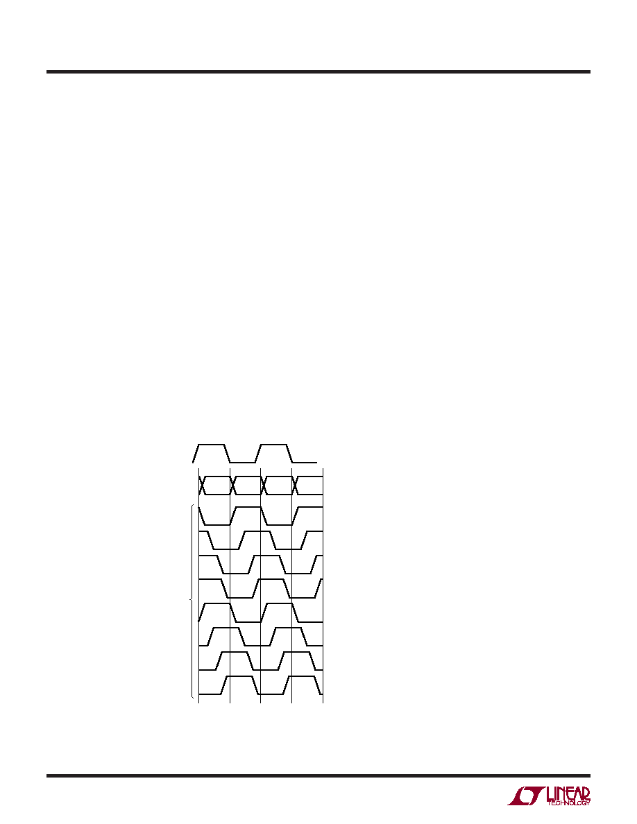
Phase Shifting the Output Clock
To allow adequate set-up and hold time when latching the
output data, the CLKOUT+ signal may need to be phase
shifted relative to the data output bits. Most FPGAs have
this feature; this is generally the best place to adjust the
timing.
Alternatively, the ADC can also phase shift the CLKOUT+/
CLKOUT– signals by serially programming mode control
register A2. The output clock can be shifted by 0°, 45°,
90°, or 135°. To use the phase shifting feature the clock
duty cycle stabilizer must be turned on. Another con-
trol register bit can invert the polarity of CLKOUT+ and
CLKOUT–, independently of the phase shift. The combina-
tion of these two features enables phase shifts of 45° up
to 315° (Figure 11).
Figure 11. Phase Shifting CLKOUT
CLKOUT+
D0-D13, OF
PHASE
SHIFT
0°
45°
90°
135°
180°
225°
270°
315°
CLKINV
0
1
CLKPHASE1
MODE CONTROL BITS
0
1
0
1
CLKPHASE0
0
1
0
1
0
1
0
1
215814 F11
ENC+
相关PDF资料 |
PDF描述 |
|---|---|
| VE-21P-IW-F1 | CONVERTER MOD DC/DC 13.8V 100W |
| LTC2175IUKG-14#PBF | IC ADC 14BIT SER 125MSPS 52-QFN |
| LTC2285IUP#PBF | IC ADC DUAL 14BIT 125MSPS 64QFN |
| VI-211-IW-F3 | CONVERTER MOD DC/DC 12V 100W |
| VI-211-IW-F2 | CONVERTER MOD DC/DC 12V 100W |
相关代理商/技术参数 |
参数描述 |
|---|---|
| LTC2158IUP-14 | 制造商:Linear Technology 功能描述:ADC DUAL 14BIT 310M 64QFN 制造商:Linear Technology 功能描述:ADC, DUAL, 14BIT, 310M, 64QFN |
| LTC2158IUP-14#PBF | 功能描述:IC ADC DUAL 14BIT 310M 64-QFN RoHS:是 类别:集成电路 (IC) >> 数据采集 - 模数转换器 系列:- 标准包装:1 系列:microPOWER™ 位数:8 采样率(每秒):1M 数据接口:串行,SPI? 转换器数目:1 功率耗散(最大):- 电压电源:模拟和数字 工作温度:-40°C ~ 125°C 安装类型:表面贴装 封装/外壳:24-VFQFN 裸露焊盘 供应商设备封装:24-VQFN 裸露焊盘(4x4) 包装:Digi-Reel® 输入数目和类型:8 个单端,单极 产品目录页面:892 (CN2011-ZH PDF) 其它名称:296-25851-6 |
| LTC2158IUP-14#TRPBF | 功能描述:IC ADC DUAL 14BIT 310M 64-QFN RoHS:是 类别:集成电路 (IC) >> 数据采集 - 模数转换器 系列:- 产品培训模块:Lead (SnPb) Finish for COTS Obsolescence Mitigation Program 标准包装:250 系列:- 位数:12 采样率(每秒):1.8M 数据接口:并联 转换器数目:1 功率耗散(最大):1.82W 电压电源:模拟和数字 工作温度:-40°C ~ 85°C 安装类型:表面贴装 封装/外壳:48-LQFP 供应商设备封装:48-LQFP(7x7) 包装:管件 输入数目和类型:2 个单端,单极 |
| LTC2159 | 制造商:LINER 制造商全称:Linear Technology 功能描述:16-Bit, 20Msps Low Power ADC |
| LTC2159CUK#PBF | 功能描述:IC ADC 16BIT PAR/SRL 20M 48-QFN RoHS:是 类别:集成电路 (IC) >> 数据采集 - 模数转换器 系列:- 标准包装:1 系列:- 位数:14 采样率(每秒):83k 数据接口:串行,并联 转换器数目:1 功率耗散(最大):95mW 电压电源:双 ± 工作温度:0°C ~ 70°C 安装类型:通孔 封装/外壳:28-DIP(0.600",15.24mm) 供应商设备封装:28-PDIP 包装:管件 输入数目和类型:1 个单端,双极 |
发布紧急采购,3分钟左右您将得到回复。