- 您现在的位置:买卖IC网 > PDF目录296329 > LTC2202CUK#TRPBF (LINEAR TECHNOLOGY CORP) 16-Bit, 10Msps ADC; Package: QFN; No of Pins: 48; Temperature Range: 0°C to +70°C PDF资料下载
参数资料
| 型号: | LTC2202CUK#TRPBF |
| 厂商: | LINEAR TECHNOLOGY CORP |
| 元件分类: | ADC |
| 英文描述: | 16-Bit, 10Msps ADC; Package: QFN; No of Pins: 48; Temperature Range: 0°C to +70°C |
| 中文描述: | 1-CH 16-BIT PROPRIETARY METHOD ADC, PARALLEL ACCESS, PQCC48 |
| 封装: | 7 X 7 MM, LEAD FREE, PLASTIC, MO-220WKKD-2, QFN-48 |
| 文件页数: | 13/32页 |
| 文件大小: | 1450K |
| 代理商: | LTC2202CUK#TRPBF |
第1页第2页第3页第4页第5页第6页第7页第8页第9页第10页第11页第12页当前第13页第14页第15页第16页第17页第18页第19页第20页第21页第22页第23页第24页第25页第26页第27页第28页第29页第30页第31页第32页
LTC2203/LTC2202
20
22032fd
the new sample is small, the charging glitch seen at the
input will be small. If the input change is large, such as
the change seen with input frequencies near Nyquist, then
a larger charging glitch will be seen.
Common Mode Bias
The ADC sample-and-hold circuit requires differential
drive to achieve specied performance. Each input may
swing ±0.625V for the 2.5V range (PGA = 0) or ±0.417V
for the 1.667V range (PGA = 1), around a common mode
voltage of 1.25V. The VCM output pin (Pin 3) is designed
to provide the common mode bias level. VCM can be tied
directly to the center tap of a transformer to set the DC
input level or as a reference level to an op amp differential
driver circuit. The VCM pin must be bypassed to ground
close to the ADC with 2.2μF or greater.
Input Drive Impedence
As with all high performance, high speed ADCs the
dynamic performance of the LTC2203/LTC2202 can be
inuenced by the input drive circuitry, particularly the
second and third harmonics. Source impedance and
input reactance can inuence SFDR. At the rising edge of
CLK the sample and hold circuit will connect the 9.1pF
sampling capacitor to the input pin and start the sampling
period. The sampling period ends when CLK falls, hold-
ing the sampled input on the sampling capacitor. Ideally,
the input circuitry should be fast enough to fully charge
the sampling capacitor during the sampling period
1/(2FCLK); however, this is not always possible and the
incomplete settling may degrade the SFDR. The sampling
glitch has been designed to be as linear as possible to
minimize the effects of incomplete settling.
For the best performance it is recomended to have a source
impedence of 100Ω or less for each input. The source
impedence should be matched for the differential inputs.
Poor matching will result in higher even order harmonics,
especially the second.
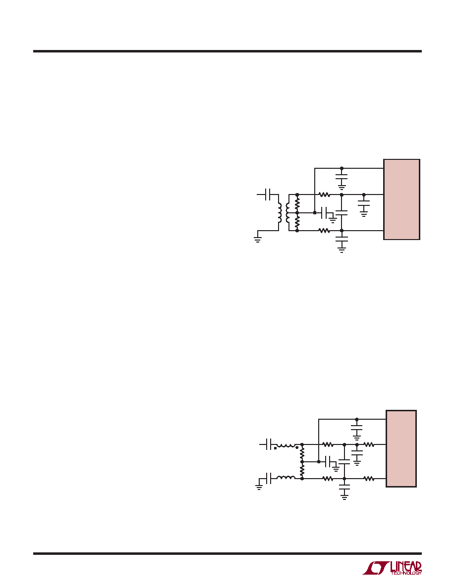
INPUT DRIVE CIRCUITS
Figure 3 shows the LTC2203/LTC2202 being driven by an RF
transformer with a center-tapped secondary. The secondary
center tap is DC biased with VCM, setting the ADC input
signal at its optimum DC level. Figure 3 shows a 1:1 turns
ratio transformer. Other turns ratios can be used; however,
as the turns ratio increases so does the impedance seen by
the ADC. Source impedance greater than 50Ω can reduce
the input bandwidth and increase high frequency distor-
tion. A disadvantage of using a transformer is the loss of
low frequency response. Most small RF transformers have
poor performance at frequencies below 1MHz.
Figure 3. Single-Ended to Differential Conversion
Using a Transformer. Recommended for Input
Frequencies from 1MHz to 100MHz
LTC2203/
LTC2202
ANALOG
INPUT
T1 = COILCRAFT WBCI-IT OR
MA/COM ETC1-1T.
RESISTORS, CAPACITORS ARE
0402 PACKAGE SIZE, EXCEPT 2.2μF.
22032 F03
0.1μF
2.2μF
12pF
0.1μF
T1
1:1
25Ω
VCM
AIN+
AIN–
Figure 4. Using a Transmission Line Balun Transformer.
Recommended for Input Frequencies from 50MHz to 250MHz
0.1μF
AIN
+
AIN
–
4.7pF
2.2μF
4.7pF
VCM
ANALOG
INPUT
0.1μF
T1
1:1
T1 = MA/COM ETC1-1-13.
RESISTORS, CAPACITORS
ARE 0402 PACKAGE SIZE,
EXCEPT 2.2F.
22032 F04
25Ω
10Ω
25Ω
LTC2203/
LTC2202
Center-tapped transformers provide a convenient means
of DC biasing the secondary; however, they often show
poor balance at high input frequencies, resulting in large
2nd order harmonics.
Figure 4 shows transformer coupling using a transmis-
sion line balun transformer. This type of transformer has
much better high frequency response and balance than ux
coupled center tap transformers. Coupling capacitors are
added at the ground and input primary terminals to allow
the secondary terminals to be biased at 1.25V.
APPLICATIONS INFORMATION
相关PDF资料 |
PDF描述 |
|---|---|
| LTC2202IUK#PBF | 16-Bit, 10Msps ADC; Package: QFN; No of Pins: 48; Temperature Range: -40°C to +85°C |
| LTC2202IUK#TRPBF | 16-Bit, 10Msps ADC; Package: QFN; No of Pins: 48; Temperature Range: -40°C to +85°C |
| LTC2203CUK#PBF | 16-Bit, 25Msps ADC; Package: QFN; No of Pins: 48; Temperature Range: 0°C to +70°C |
| LTC2203CUK#TRPBF | 16-Bit, 25Msps ADC; Package: QFN; No of Pins: 48; Temperature Range: 0°C to +70°C |
| LTC2203IUK#PBF | 16-Bit, 25Msps ADC; Package: QFN; No of Pins: 48; Temperature Range: -40°C to +85°C |
相关代理商/技术参数 |
参数描述 |
|---|---|
| LTC2202IUK | 制造商:Linear Technology 功能描述:ADC Single Pipelined 10Msps 16-bit Parallel 48-Pin QFN EP |
| LTC2202IUK#PBF | 功能描述:IC ADC 16-BIT 10MSPS 48-QFN RoHS:是 类别:集成电路 (IC) >> 数据采集 - 模数转换器 系列:- 标准包装:1 系列:microPOWER™ 位数:8 采样率(每秒):1M 数据接口:串行,SPI? 转换器数目:1 功率耗散(最大):- 电压电源:模拟和数字 工作温度:-40°C ~ 125°C 安装类型:表面贴装 封装/外壳:24-VFQFN 裸露焊盘 供应商设备封装:24-VQFN 裸露焊盘(4x4) 包装:Digi-Reel® 输入数目和类型:8 个单端,单极 产品目录页面:892 (CN2011-ZH PDF) 其它名称:296-25851-6 |
| LTC2202IUK#TRPBF | 功能描述:IC ADC 16-BIT 10MSPS 48-QFN RoHS:是 类别:集成电路 (IC) >> 数据采集 - 模数转换器 系列:- 标准包装:1 系列:- 位数:14 采样率(每秒):83k 数据接口:串行,并联 转换器数目:1 功率耗散(最大):95mW 电压电源:双 ± 工作温度:0°C ~ 70°C 安装类型:通孔 封装/外壳:28-DIP(0.600",15.24mm) 供应商设备封装:28-PDIP 包装:管件 输入数目和类型:1 个单端,双极 |
| LTC2202UK | 制造商:LINER 制造商全称:Linear Technology 功能描述:16-Bit, 25Msps/10Msps ADCs |
| LTC2203 | 制造商:LINER 制造商全称:Linear Technology 功能描述:16-Bit, 25Msps/10Msps ADCs |
发布紧急采购,3分钟左右您将得到回复。