- 您现在的位置:买卖IC网 > PDF目录39413 > LTC2203C#TRPBF (LINEAR TECHNOLOGY CORP) 1-CH 16-BIT PROPRIETARY METHOD ADC, PARALLEL ACCESS, PQCC48 PDF资料下载
参数资料
| 型号: | LTC2203C#TRPBF |
| 厂商: | LINEAR TECHNOLOGY CORP |
| 元件分类: | ADC |
| 英文描述: | 1-CH 16-BIT PROPRIETARY METHOD ADC, PARALLEL ACCESS, PQCC48 |
| 封装: | 7 X 7 MM, LEAD FREE, PLASTIC, MO-220-WKKD-2, QFN-48 |
| 文件页数: | 11/26页 |
| 文件大小: | 1118K |
| 代理商: | LTC2203C#TRPBF |
LTC2203/LTC2202
19
22032p
the new sample is small, the charging glitch seen at the
input will be small. If the input change is large, such as
the change seen with input frequencies near Nyquist, then
a larger charging glitch will be seen.
Common Mode Bias
The ADC sample-and-hold circuit requires differential
drive to achieve specied performance. Each input may
swing ±0.625V for the 2.5V range (PGA = 0) or ±0.417V
for the 1.667V range (PGA = 1), around a common mode
voltage of 1.25V. The VCM output pin (Pin 3) is designed
to provide the common mode bias level. VCM can be tied
directly to the center tap of a transformer to set the DC
input level or as a reference level to an op amp differential
driver circuit. The VCM pin must be bypassed to ground
close to the ADC with 2.2F or greater.
Input Drive Impedence
As with all high performance, high speed ADCs the
dynamic performance of the LTC2203/LTC2202 can be
inuenced by the input drive circuitry, particularly the
second and third harmonics. Source impedance and
input reactance can inuence SFDR. At the rising edge of
CLK the sample and hold circuit will connect the 9.1pF
sampling capacitor to the input pin and start the sampling
period. The sampling period ends when CLK falls, hold-
ing the sampled input on the sampling capacitor. Ideally,
the input circuitry should be fast enough to fully charge
the sampling capacitor during the sampling period
1/(2FCLK); however, this is not always possible and the
incomplete settling may degrade the SFDR. The sampling
glitch has been designed to be as linear as possible to
minimize the effects of incomplete settling.
Forthebestperformanceitisrecomendedtohaveasource
impedence of 100Ω or less for each input. The source
impedence should be matched for the differential inputs.
Poor matching will result in higher even order harmonics,
especially the second.
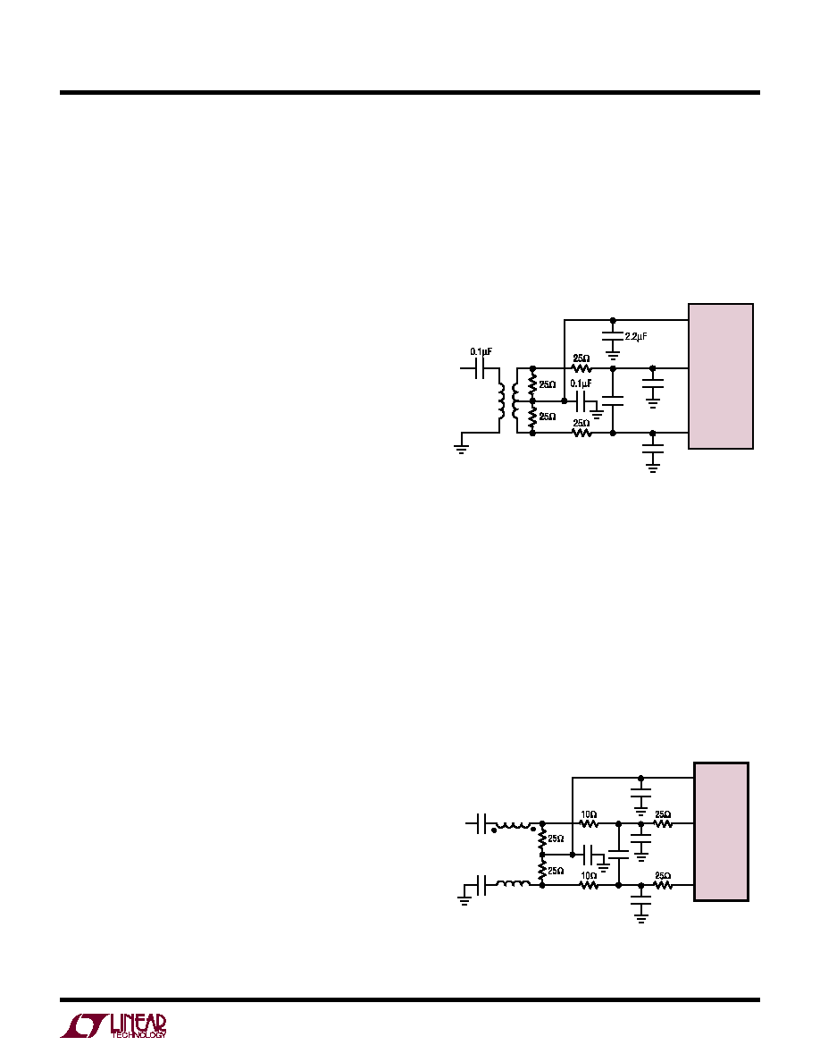
INPUT DRIVE CIRCUITS
Figure 3 shows the LTC2203/LTC2202 being driven by
an RF transformer with a center-tapped secondary. The
secondary center tap is DC biased with VCM, setting the
ADC input signal at its optimum DC level. Figure 3 shows
a 1:1 turns ratio transformer. Other turns ratios can be
used; however, as the turns ratio increases so does the
impedance seen by the ADC. Source impedance greater
than 50Ω can reduce the input bandwidth and increase
high frequency distortion. A disadvantage of using a
transformer is the loss of low frequency response. Most
small RF transformers have poor performance at frequen-
cies below 1MHz.
Center-tapped transformers provide a convenient means
of DC biasing the secondary; however, they often show
poor balance at high input frequencies, resulting in large
2nd order harmonics.
Figure 4 shows transformer coupling using a transmis-
sion line balun transformer. This type of transformer has
muchbetterhighfrequencyresponseandbalancethanux
coupled center tap transformers. Coupling capacitors are
added at the ground and input primary terminals to allow
the secondary terminals to be biased at 1.25V.
APPLICATIO S I FOR ATIO
W
U
Figure 3. Single-Ended to Differential Conversion
Using a Transformer. Recommended for Input
Frequencies from 1MHz to 50MHz
AIN+
AIN–
12pF
VCM
LTC2203/02
ANALOG
INPUT
T1
1:1
T1 = COILCRAFT WBCI-IT OR
MA/COM ETC1-1T, RESISTORS,
CAPACITORS ARE 0402 PACKAGE
SIZE EXCEPT 2.2
F
22032 F03
Figure 4. Using a Transmission Line Balun Transformer.
Recommended for Input Frequencies from 50MHz to 250MHz
0.1
F
AIN+
AIN–
4.7pF
2.2
F
4.7pF
VCM
LTC2203/02
ANALOG
INPUT
0.1
F
0.1
F
T1
1:1
T1 = MA/COM ETC1-1-13
RESISTORS, CAPACITORS
ARE 0402 PACKAGE SIZE
EXCEPT 2.2F
22032 F04
相关PDF资料 |
PDF描述 |
|---|---|
| LTC2203C#TR | 1-CH 16-BIT PROPRIETARY METHOD ADC, PARALLEL ACCESS, PQCC48 |
| LTC2203C | 1-CH 16-BIT PROPRIETARY METHOD ADC, PARALLEL ACCESS, PQCC48 |
| LTC2203I#TRPBF | 1-CH 16-BIT PROPRIETARY METHOD ADC, PARALLEL ACCESS, PQCC48 |
| LTC2203I#TR | 1-CH 16-BIT PROPRIETARY METHOD ADC, PARALLEL ACCESS, PQCC48 |
| LTC2202C#PBF | 1-CH 16-BIT PROPRIETARY METHOD ADC, PARALLEL ACCESS, PQCC48 |
相关代理商/技术参数 |
参数描述 |
|---|---|
| LTC2203CUK | 制造商:Linear Technology 功能描述:ADC Single Pipelined 25Msps 16-bit Parallel 48-Pin QFN EP |
| LTC2203CUK#PBF | 制造商:Linear Technology 功能描述:ADC Single Pipelined 25Msps 16-bit Parallel 48-Pin QFN EP 制造商:Linear Technology 功能描述:Single ADC Pipelined 25Msps 16-bit Parallel 48-Pin QFN EP 制造商:Linear Technology 功能描述:IC ADC 16-BIT 25MSPS 48-QFN 制造商:Linear Technology 功能描述:IC, ADC, 16BIT, 25MSPS, QFN-48, Resolution (Bits):16bit, Sampling Rate:25MSPS, Supply Voltage Type:Single, Supply Voltage Min:3.135V, Supply Voltage Max:3.465V, Supply Current:66mA, Digital IC Case Style:QFN, No. of Pins:48 , RoHS Compliant: Yes 制造商:Linear Technology 功能描述:MS-ADC/High Speed, 16-bit, 25Msps ADC |
| LTC2203CUK#TRPBF | 制造商:Linear Technology 功能描述:ADC Single Pipelined 25Msps 16-bit Parallel 48-Pin QFN EP T/R 制造商:Linear Technology 功能描述:IC ADC 16-BIT 25MSPS 48-QFN |
| LTC2203IUK | 制造商:Linear Technology 功能描述:Single ADC Pipelined 25Msps 16-bit Parallel 48-Pin QFN EP |
| LTC2203IUK#PBF | 制造商:Linear Technology 功能描述:ADC Single Pipelined 25Msps 16-bit Parallel 48-Pin QFN EP 制造商:Linear Technology 功能描述:Single ADC Pipelined 25Msps 16-bit Parallel 48-Pin QFN EP 制造商:Linear Technology 功能描述:IC ADC 16-BIT 25MSPS 48-QFN 制造商:Linear Technology 功能描述:IC ADC 16BIT 25MSPS QFN-48 制造商:Linear Technology 功能描述:IC, ADC, 16BIT, 25MSPS, QFN-48, Resolution (Bits):16bit, Sampling Rate:25MSPS, Supply Voltage Type:Single, Supply Voltage Min:3.135V, Supply Voltage Max:3.465V, Supply Current:66mA, Digital IC Case Style:QFN, No. of Pins:48 , RoHS Compliant: Yes 制造商:Linear Technology 功能描述:MS-ADC/High Speed, 16-bit, 25Msps ADC |
发布紧急采购,3分钟左右您将得到回复。