- 您现在的位置:买卖IC网 > PDF目录296330 > LTC2207IUK#PBF (LINEAR TECHNOLOGY CORP) 16-Bit, 105Msps ADC; Package: QFN; No of Pins: 48; Temperature Range: -40°C to +85°C PDF资料下载
参数资料
| 型号: | LTC2207IUK#PBF |
| 厂商: | LINEAR TECHNOLOGY CORP |
| 元件分类: | ADC |
| 英文描述: | 16-Bit, 105Msps ADC; Package: QFN; No of Pins: 48; Temperature Range: -40°C to +85°C |
| 中文描述: | 1-CH 16-BIT PROPRIETARY METHOD ADC, PARALLEL ACCESS, PQCC48 |
| 封装: | 7 X 7 MM, LEAD FREE, PLASTIC, MO-220WKKD-2, QFN-48 |
| 文件页数: | 16/32页 |
| 文件大小: | 1270K |
| 代理商: | LTC2207IUK#PBF |
第1页第2页第3页第4页第5页第6页第7页第8页第9页第10页第11页第12页第13页第14页第15页当前第16页第17页第18页第19页第20页第21页第22页第23页第24页第25页第26页第27页第28页第29页第30页第31页第32页
LTC2207/LTC2206
23
22076fc
DIGITAL OUTPUTS
Digital Output Buffers
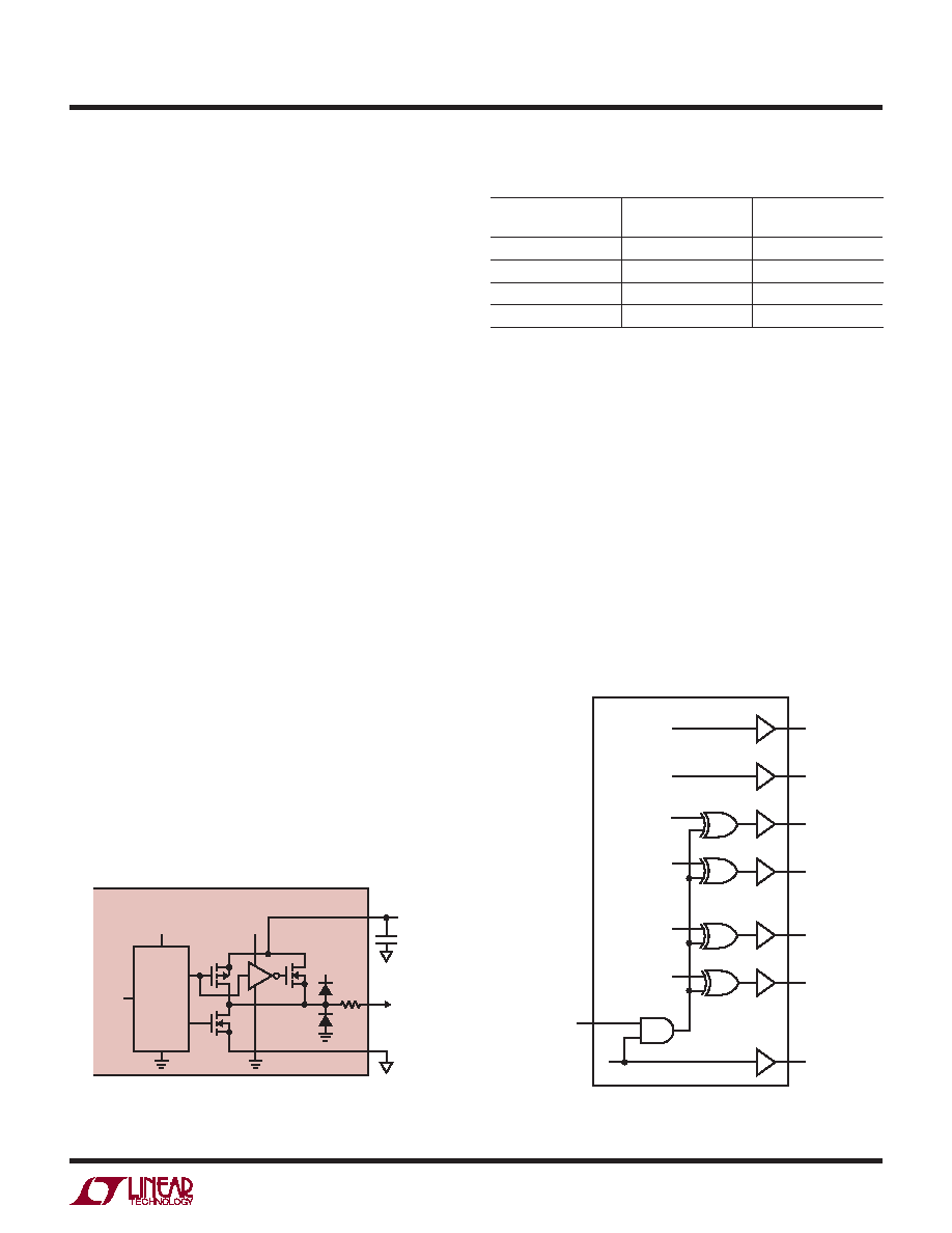
Figure 11 shows an equivalent circuit for a single output
buffer. Each buffer is powered by OVDD and OGND, isolated
from the ADC power and ground. The additional N-channel
transistor in the output driver allows operation down to
low voltages. The internal resistor in series with the output
eliminates the need for external damping resistors.
As with all high speed/high resolution converters, the digi-
tal output loading can affect the performance. The digital
outputs of the LTC2207/LTC2206 should drive a minimum
capacitive load to avoid possible interaction between the
digital outputs and sensitive input circuitry. The output
should be buffered with a device such as a ALVCH16373
CMOS latch. For full speed operation the capacitive load
should be kept under 10pF. A resistor in series with the
output may be used but is not required since the output
buffer has a series resistor of 33
Ω on chip.
Lower OVDD voltages will also help reduce interference
from the digital outputs.
Data Format
The LTC2207/LTC2206 parallel digital output can be
selected for offset binary or 2’s complement format. The
format is selected with the MODE pin. This pin has a four
level logic input, centered at 0, 1/3VDD, 2/3VDD and VDD.
An external resistor divider can be user to set the 1/3VDD
and 2/3VDD logic levels. Table 1 shows the logic states
for the MODE pin.
LTC2207/LTC2206
22076 F11
OVDD
VDD
0.1μF
TYPICAL
DATA
OUTPUT
OGND
OVDD
0.5V
TO 3.6V
PREDRIVER
LOGIC
DATA
FROM
LATCH
33Ω
Figure 11. Equivalent Circuit for a Digital Output Buffer
Table 1. MODE Pin Function
MODE
Output Format
Clock Duty
Cycle Stabilizer
0(GND)
Offset Binary
Off
1/3VDD
Offset Binary
On
2/3VDD
2’s Complement
On
VDD
2’s Complement
Off
Overow Bit
An overow output bit (OF) indicates when the converter
is over-ranged or under-ranged. A logic high on the OF
pin indicates an overow or underow.
Output Clock
The ADC has a delayed version of the encode input available
as a digital output. Both a noninverted version, CLKOUT+
and an inverted version CLKOUT– are provided. The
CLKOUT+/CLKOUT– can be used to synchronize the con-
verter data to the digital system. This is necessary when
using a sinusoidal encode. Data can be latched on the
rising edge of CLKOUT+ or the falling edge of CLKOUT–.
CLKOUT+ falls and CLKOUT– rises as the data outputs
are updated.
Figure 12. Functional Equivalent of Digital Output Randomizer
CLKOUT+
OF
D15/D0
D14/D0
D2/D0
D1/D0
D0
D1
RAND = HIGH,
SCRAMBLE
ENABLED
D2
D14
D15
OF
LTC2207/LTC2206
CLKOUT
RAND
22076 F12
APPLICATIONS INFORMATION
相关PDF资料 |
PDF描述 |
|---|---|
| LTC2207IUK#TRPBF | 16-Bit, 105Msps ADC; Package: QFN; No of Pins: 48; Temperature Range: -40°C to +85°C |
| LTC2208CUP-14#PBF | 16-Bit, 130Msps ADC; Package: QFN; No of Pins: 64; Temperature Range: 0°C to +70°C |
| LTC2208CUP#PBF | 16-Bit, 130Msps ADC; Package: QFN; No of Pins: 64; Temperature Range: 0°C to +70°C |
| LTC2208CUP#TRPBF | 16-Bit, 130Msps ADC; Package: QFN; No of Pins: 64; Temperature Range: 0°C to +70°C |
| LTC2411CMS | Analog-to-Digital Converter, 24-Bit |
相关代理商/技术参数 |
参数描述 |
|---|---|
| LTC2207UK | 制造商:LINER 制造商全称:Linear Technology 功能描述:16-Bit, 105Msps/80Msps ADCs |
| LTC2207UK-14 | 制造商:LINER 制造商全称:Linear Technology 功能描述:14-Bit, 105Msps/80Msps ADCs |
| LTC2208 | 制造商:LINER 制造商全称:Linear Technology 功能描述:Dual 14-Bit 250Msps |
| LTC2208-14 | 制造商:LINER 制造商全称:Linear Technology 功能描述:14-Bit, 130Msps ADC |
| LTC2208CUP | 制造商:Linear Technology 功能描述:IC ADC 16BIT 130MSPS 64-QFN |
发布紧急采购,3分钟左右您将得到回复。