- 您现在的位置:买卖IC网 > PDF目录296330 > LTC2207IUK#PBF (LINEAR TECHNOLOGY CORP) 16-Bit, 105Msps ADC; Package: QFN; No of Pins: 48; Temperature Range: -40°C to +85°C PDF资料下载
参数资料
| 型号: | LTC2207IUK#PBF |
| 厂商: | LINEAR TECHNOLOGY CORP |
| 元件分类: | ADC |
| 英文描述: | 16-Bit, 105Msps ADC; Package: QFN; No of Pins: 48; Temperature Range: -40°C to +85°C |
| 中文描述: | 1-CH 16-BIT PROPRIETARY METHOD ADC, PARALLEL ACCESS, PQCC48 |
| 封装: | 7 X 7 MM, LEAD FREE, PLASTIC, MO-220WKKD-2, QFN-48 |
| 文件页数: | 17/32页 |
| 文件大小: | 1270K |
| 代理商: | LTC2207IUK#PBF |
第1页第2页第3页第4页第5页第6页第7页第8页第9页第10页第11页第12页第13页第14页第15页第16页当前第17页第18页第19页第20页第21页第22页第23页第24页第25页第26页第27页第28页第29页第30页第31页第32页
LTC2207/LTC2206
24
22076fc
APPLICATIONS INFORMATION
Digital Output Randomizer
Interference from the ADC digital outputs is sometimes
unavoidable. Interference from the digital outputs may be
from capacitive or inductive coupling or coupling through
the ground plane. Even a tiny coupling factor can result in
discernible unwanted tones in the ADC output spectrum.
By randomizing the digital output before it is transmitted
off chip, these unwanted tones can be randomized, trading
a slight increase in the noise oor for a large reduction in
unwanted tone amplitude.
The digital output is “Randomized” by applying an exclu-
sive-OR logic operation between the LSB and all other data
output bits. To decode, the reverse operation is applied;
that is, an exclusive-OR operation is applied between the
LSB and all other bits. The LSB, OF and CLKOUT outputs
are not affected. The output Randomizer function is active
when the RAND pin is high.
Output Driver Power
Separate output power and ground pins allow the output
drivers to be isolated from the analog circuitry. The power
supply for the digital output buffers, OVDD, should be tied
to the same power supply as for the logic being driven.
For example, if the converter is driving a DSP powered
by a 1.8V supply, then OVDD should be tied to that same
1.8V supply. In CMOS mode OVDD can be powered with
any logic voltage up to the VDD of the ADC. OGND can be
powered with any voltage from ground up to 1V and must
be less than OVDD. The logic outputs will swing between
OGND and OVDD.
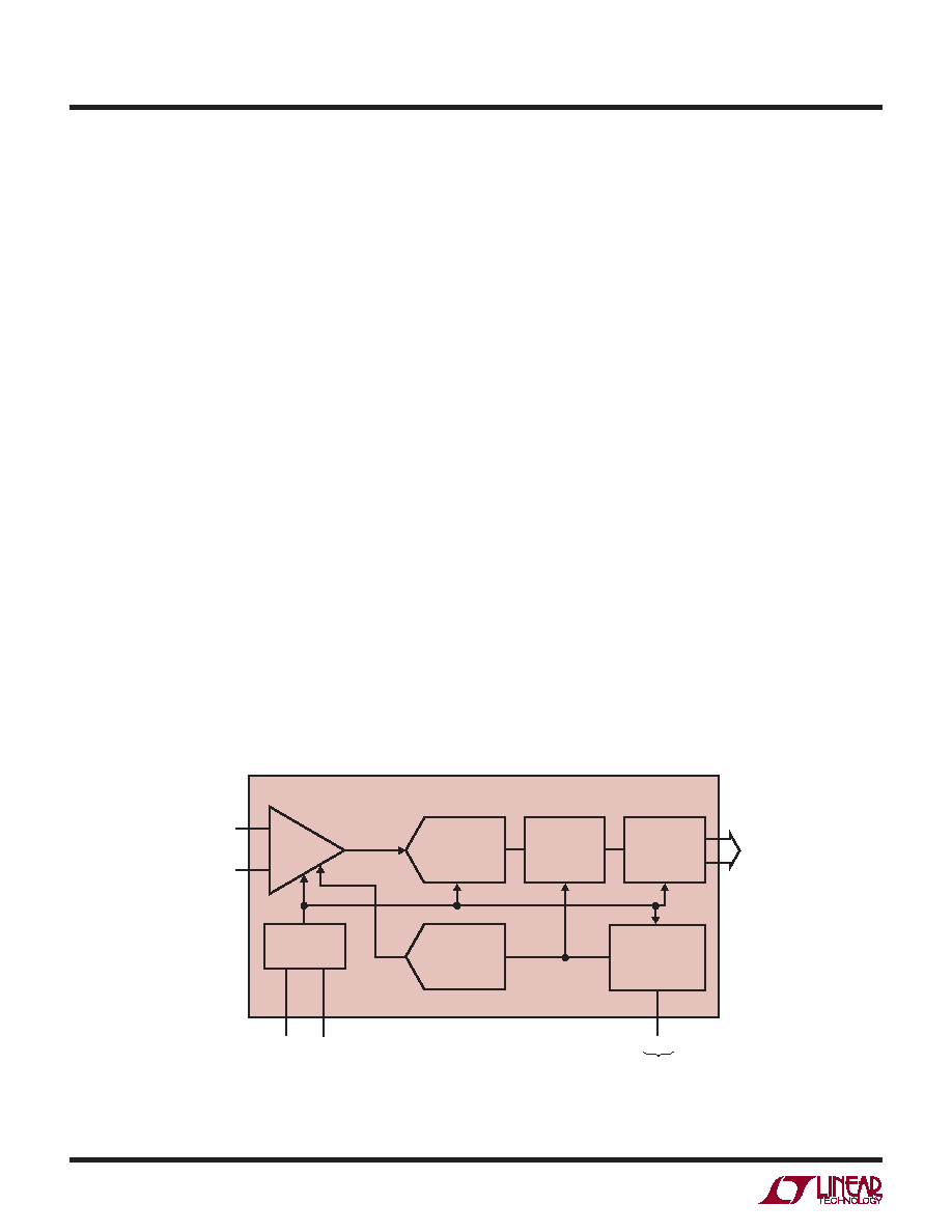
Internal Dither
The LTC2207/LTC2206 are 16-bit ADCs with a very linear
transfer function; however, at low input levels even slight
imperfections in the transfer function will result in unwanted
tones. Small errors in the transfer function are usually a
result of ADC element mismatches. An optional internal
dither mode can be enabled to randomize the input location
on the ADC transfer curve, resulting in improved SFDR
for low signal levels.
As shown in Figure 15, the output of the sample-and-hold
amplier is summed with the output of a dither DAC. The
dither DAC is driven by a long sequence pseudo-random
number generator; the random number fed to the dither
DAC is also subtracted from the ADC result. If the dither
DAC is precisely calibrated to the ADC, very little of the
dither signal will be seen at the output. The dither signal
that does leak through will appear as white noise. The dither
DAC is calibrated to result in less than 0.5dB elevation in
the noise oor of the ADC, as compared to the noise oor
with dither off.
Figure 13. Functional Equivalent Block Diagram of Internal Dither Circuit
+–
AIN–
AIN+
S/H
AMP
DIGITAL
SUMMATION
OUTPUT
DRIVERS
MULTIBIT DEEP
PSEUDO-RANDOM
NUMBER
GENERATOR
16-BIT
PIPELINED
ADC CORE
PRECISION
DAC
CLOCK/DUTY
CYCLE
CONTROL
CLKOUT
OF
D15
D0
ENC
DITHER ENABLE
HIGH = DITHER ON
LOW = DITHER OFF
DITH
ENC
ANALOG
INPUT
22076 F13
LTC2207/LTC2206
相关PDF资料 |
PDF描述 |
|---|---|
| LTC2207IUK#TRPBF | 16-Bit, 105Msps ADC; Package: QFN; No of Pins: 48; Temperature Range: -40°C to +85°C |
| LTC2208CUP-14#PBF | 16-Bit, 130Msps ADC; Package: QFN; No of Pins: 64; Temperature Range: 0°C to +70°C |
| LTC2208CUP#PBF | 16-Bit, 130Msps ADC; Package: QFN; No of Pins: 64; Temperature Range: 0°C to +70°C |
| LTC2208CUP#TRPBF | 16-Bit, 130Msps ADC; Package: QFN; No of Pins: 64; Temperature Range: 0°C to +70°C |
| LTC2411CMS | Analog-to-Digital Converter, 24-Bit |
相关代理商/技术参数 |
参数描述 |
|---|---|
| LTC2207UK | 制造商:LINER 制造商全称:Linear Technology 功能描述:16-Bit, 105Msps/80Msps ADCs |
| LTC2207UK-14 | 制造商:LINER 制造商全称:Linear Technology 功能描述:14-Bit, 105Msps/80Msps ADCs |
| LTC2208 | 制造商:LINER 制造商全称:Linear Technology 功能描述:Dual 14-Bit 250Msps |
| LTC2208-14 | 制造商:LINER 制造商全称:Linear Technology 功能描述:14-Bit, 130Msps ADC |
| LTC2208CUP | 制造商:Linear Technology 功能描述:IC ADC 16BIT 130MSPS 64-QFN |
发布紧急采购,3分钟左右您将得到回复。