参数资料
| 型号: | LTC2231IUP#TRPBF |
| 厂商: | Linear Technology |
| 文件页数: | 13/32页 |
| 文件大小: | 0K |
| 描述: | IC ADC 10BIT 135MSPS 64-QFN |
| 标准包装: | 2,000 |
| 位数: | 10 |
| 采样率(每秒): | 135M |
| 数据接口: | 并联 |
| 转换器数目: | 1 |
| 功率耗散(最大): | 924mW |
| 电压电源: | 单电源 |
| 工作温度: | -40°C ~ 85°C |
| 安装类型: | 表面贴装 |
| 封装/外壳: | 64-WFQFN 裸露焊盘 |
| 供应商设备封装: | 64-QFN(9x9) |
| 包装: | 带卷 (TR) |
| 输入数目和类型: | 1 个单端,双极; 1 个差分,双极 |
第1页第2页第3页第4页第5页第6页第7页第8页第9页第10页第11页第12页当前第13页第14页第15页第16页第17页第18页第19页第20页第21页第22页第23页第24页第25页第26页第27页第28页第29页第30页第31页第32页
LTC2230/LTC2231
20
22301fb
60) may be used to provide the common mode bias level.
VCM can be tied directly to the center tap of a transformer
to set the DC input level or as a reference level to an op amp
differential driver circuit. The VCM pin must be bypassed to
ground close to the ADC with a 2.2
μF or greater capacitor.
Input Drive Impedance
As with all high performance, high speed ADCs, the
dynamic performance of the LTC2230/LTC2231 can be
influenced by the input drive circuitry, particularly the
second and third harmonics. Source impedance and input
reactance can influence SFDR. At the falling edge of ENC,
the sample-and-hold circuit will connect the 1.6pF sam-
pling capacitor to the input pin and start the sampling
period. The sampling period ends when ENC rises, holding
the sampled input on the sampling capacitor. Ideally the
input circuitry should be fast enough to fully charge
the sampling capacitor during the sampling period
1/(2FENCODE); however, this is not always possible and the
incomplete settling may degrade the SFDR. The sampling
glitch has been designed to be as linear as possible to
minimize the effects of incomplete settling.
For the best performance, it is recommended to have a
source impedance of 100
Ω or less for each input. The
source impedance should be matched for the differential
inputs. Poor matching will result in higher even order
harmonics, especially the second.
Input Drive Circuits
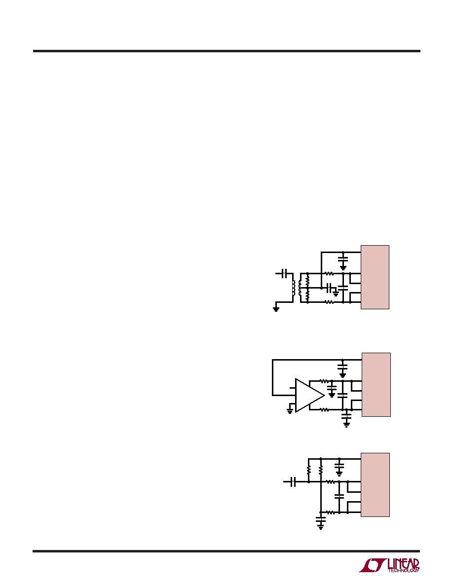
Figure 3 shows the LTC2230/LTC2231 being driven by an
RF transformer with a center tapped secondary. The
secondary center tap is DC biased with VCM, setting the
ADC input signal at its optimum DC level. Terminating on
the transformer secondary is desirable, as this provides a
common mode path for charging glitches caused by the
sample and hold. Figure 3 shows a 1:1 turns ratio trans-
former. Other turns ratios can be used if the source
impedance seen by the ADC does not exceed 100
Ω for
each ADC input. A disadvantage of using a transformer is
the loss of low frequency response. Most small RF trans-
formers have poor performance at frequencies below
1MHz.
Figure 4 demonstrates the use of a differential amplifier to
convert a single ended input signal into a differential input
signal. The advantage of this method is that it provides low
frequency input response; however, the limited gain band-
width of most op amps will limit the SFDR at high input
frequencies.
Figure 5 shows a single-ended input circuit. The imped-
ance seen by the analog inputs should be matched. This
circuit is not recommended if low distortion is required.
The 25
Ωresistorsand12pFcapacitorontheanaloginputs
serve two purposes: isolating the drive circuitry from the
sample-and-hold charging glitches and limiting the
wideband noise at the converter input. For input frequen-
cies higher than 100MHz, the capacitor may need to be
decreased to prevent excessive signal loss.
Figure 3. Single-Ended to Differential
Conversion Using a Transformer
Figure 4. Differential Drive with an Amplifier
APPLICATIO S I FOR ATIO
WU
UU
Figure 5. Single-Ended Drive
25
Ω
25
Ω
25
Ω
25
Ω
0.1
μF
AIN
+
AIN
+
AIN
–
AIN
–
12pF
2.2
μF
VCM
LTC2230/
LTC2231
ANALOG
INPUT
0.1
μFT1
1:1
T1 = MA/COM ETC1-1T
RESISTORS, CAPACITORS
ARE 0402 PACKAGE SIZE
22301 F03
25
Ω
25
Ω
AIN
+
AIN
+
AIN
–
AIN
–
12pF
2.2
μF
3pF
VCM
LTC2230/
LTC2231
22301 F04
–
+
CM
ANALOG
INPUT
HIGH SPEED
DIFFERENTIAL
AMPLIFIER
AMPLIFIER = LTC6600-20, AD8138, ETC.
25
Ω
0.1
μF
ANALOG
INPUT
VCM
AIN
+
AIN
+
AIN
–
AIN
–
1k
12pF
22301 F05
2.2
μF
1k
25
Ω
0.1
μF
LTC2230/
LTC2231
相关PDF资料 |
PDF描述 |
|---|---|
| LTC2233CUK#TRPBF | IC ADC 10BIT 80MSPS SAMPL 48QFN |
| LTC2234IUK#TRPBF | IC ADC 10BIT 135MSPS SAMPL 48QFN |
| LTC2237IUH#TRPBF | IC ADC 10BIT 40MSPS 3V 32-QFN |
| LTC2239CUH#PBF | IC ADC 10-BIT 80MSPS 3V 32-QFN |
| LTC2240CUP-12#PBF | IC ADC 12BIT 170MSPS 64-QFN |
相关代理商/技术参数 |
参数描述 |
|---|---|
| LTC2231UP | 制造商:LINER 制造商全称:Linear Technology 功能描述:10-Bit,170Msps/135Msps ADCs |
| LTC2232 | 制造商:LINER 制造商全称:Linear Technology 功能描述:14-Bit, 80Msps Low Power 3V ADC |
| LTC2232CUK | 功能描述:IC ADC 10BIT 105MSPS SAMPL 48QFN RoHS:否 类别:集成电路 (IC) >> 数据采集 - 模数转换器 系列:- 标准包装:1,000 系列:- 位数:12 采样率(每秒):300k 数据接口:并联 转换器数目:1 功率耗散(最大):75mW 电压电源:单电源 工作温度:0°C ~ 70°C 安装类型:表面贴装 封装/外壳:24-SOIC(0.295",7.50mm 宽) 供应商设备封装:24-SOIC 包装:带卷 (TR) 输入数目和类型:1 个单端,单极;1 个单端,双极 |
| LTC2232CUK#PBF | 功能描述:IC ADC 10BIT 105MSPS SAMPL 48QFN RoHS:是 类别:集成电路 (IC) >> 数据采集 - 模数转换器 系列:- 标准包装:1,000 系列:- 位数:12 采样率(每秒):300k 数据接口:并联 转换器数目:1 功率耗散(最大):75mW 电压电源:单电源 工作温度:0°C ~ 70°C 安装类型:表面贴装 封装/外壳:24-SOIC(0.295",7.50mm 宽) 供应商设备封装:24-SOIC 包装:带卷 (TR) 输入数目和类型:1 个单端,单极;1 个单端,双极 |
| LTC2232CUK#TR | 功能描述:IC ADC 10BIT 105MSPS SAMPL 48QFN RoHS:否 类别:集成电路 (IC) >> 数据采集 - 模数转换器 系列:- 标准包装:1,000 系列:- 位数:12 采样率(每秒):300k 数据接口:并联 转换器数目:1 功率耗散(最大):75mW 电压电源:单电源 工作温度:0°C ~ 70°C 安装类型:表面贴装 封装/外壳:24-SOIC(0.295",7.50mm 宽) 供应商设备封装:24-SOIC 包装:带卷 (TR) 输入数目和类型:1 个单端,单极;1 个单端,双极 |
发布紧急采购,3分钟左右您将得到回复。