参数资料
| 型号: | LTC2231IUP#TRPBF |
| 厂商: | Linear Technology |
| 文件页数: | 17/32页 |
| 文件大小: | 0K |
| 描述: | IC ADC 10BIT 135MSPS 64-QFN |
| 标准包装: | 2,000 |
| 位数: | 10 |
| 采样率(每秒): | 135M |
| 数据接口: | 并联 |
| 转换器数目: | 1 |
| 功率耗散(最大): | 924mW |
| 电压电源: | 单电源 |
| 工作温度: | -40°C ~ 85°C |
| 安装类型: | 表面贴装 |
| 封装/外壳: | 64-WFQFN 裸露焊盘 |
| 供应商设备封装: | 64-QFN(9x9) |
| 包装: | 带卷 (TR) |
| 输入数目和类型: | 1 个单端,双极; 1 个差分,双极 |
第1页第2页第3页第4页第5页第6页第7页第8页第9页第10页第11页第12页第13页第14页第15页第16页当前第17页第18页第19页第20页第21页第22页第23页第24页第25页第26页第27页第28页第29页第30页第31页第32页
LTC2230/LTC2231
24
22301fb
as 50
Ω to external circuitry and may eliminate the need for
external damping resistors.
As with all high speed/high resolution converters, the
digital output loading can affect the performance. The
digital outputs of the LTC2230/LTC2231 should drive a
minimal capacitive load to avoid possible interaction be-
tween the digital outputs and sensitive input circuitry. The
output should be buffered with a device such as an
ALVCH16373 CMOS latch. For full speed operation the
capacitive load should be kept under 10pF.
Lower OVDD voltages will also help reduce interference
from the digital outputs.
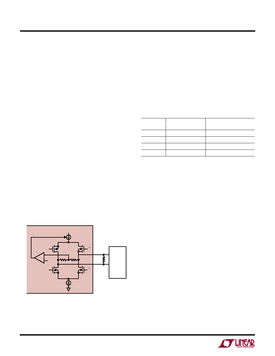
Digital Output Buffers (LVDS Mode)
Figure 13b shows an equivalent circuit for a differential
output pair in the LVDS output mode. A 3.5mA current is
steered from OUT+ to OUT– or vice versa which creates a
±350mV differential voltage across the 100Ω termination
resistor at the LVDS receiver. A feedback loop regulates
the common mode output voltage to 1.25V. For proper
operation each LVDS output pair needs an external 100
Ω
termination resistor, even if the signal is not used (such as
OF+/OF– or CLKOUT+/CLKOUT–). To minimize noise the
PC board traces for each LVDS output pair should be
routed close together. To minimize clock skew all LVDS PC
board traces should have about the same length.
APPLICATIO S I FOR ATIO
WU
UU
Data Format
The LTC2230/LTC2231 parallel digital output can be se-
lected for offset binary or 2’s complement format. The
format is selected with the MODE pin. Connecting MODE
to GND or 1/3VDD selects offset binary output format.
Connecting MODE to 2/3VDD or VDD selects 2’s comple-
ment output format. An external resistor divider can be
used to set the 1/3VDD or 2/3VDD logic values. Table 3
shows the logic states for the MODE pin.
LTC2230/LTC2231
22301 F13b
OVDD
LVDS
RECEIVER
OGND
1.25V
D
OUT+
OUT–
100
Ω
+
–
3.5mA
10k
Figure 13b. Digital Output in LVDS Mode
Table 3. MODE Pin Function
Clock Duty
MODE Pin
Output Format
Cycle Stablizer
0
Offset Binary
Off
1/3VDD
Offset Binary
On
2/3VDD
2’s Complement
On
VDD
2’s Complement
Off
Overflow Bit
An overflow output bit indicates when the converter is
overranged or underranged. In CMOS mode, a logic high
on the OFA pin indicates an overflow or underflow on the
A data bus, while a logic high on the OFB pin indicates an
overflow or underflow on the B data bus. In LVDS mode,
a differential logic high on the OF+/OF– pins indicates an
overflow or underflow.
Output Clock
The ADC has a delayed version of the ENC+ input available
as a digital output, CLKOUT. The CLKOUT pin can be used
to synchronize the converter data to the digital system. This
is necessary when using a sinusoidal encode. In all CMOS
modes, A bus data will be updated just after CLKOUTA rises
and can be latched on the falling edge of CLKOUTA. In demux
CMOS mode with interleaved update, B bus data will be
updated just after CLKOUTB rises and can be latched on the
falling edge of CLKOUTB. In demux CMOS mode with si-
multaneous update, B bus data will be updated just after
CLKOUTB falls and can be latched on the rising edge of
CLKOUTB. In LVDS mode, data will be updated just after
CLKOUT+/CLKOUT– rises and can be latched on the falling
edge of CLKOUT+/CLKOUT–.
相关PDF资料 |
PDF描述 |
|---|---|
| LTC2233CUK#TRPBF | IC ADC 10BIT 80MSPS SAMPL 48QFN |
| LTC2234IUK#TRPBF | IC ADC 10BIT 135MSPS SAMPL 48QFN |
| LTC2237IUH#TRPBF | IC ADC 10BIT 40MSPS 3V 32-QFN |
| LTC2239CUH#PBF | IC ADC 10-BIT 80MSPS 3V 32-QFN |
| LTC2240CUP-12#PBF | IC ADC 12BIT 170MSPS 64-QFN |
相关代理商/技术参数 |
参数描述 |
|---|---|
| LTC2231UP | 制造商:LINER 制造商全称:Linear Technology 功能描述:10-Bit,170Msps/135Msps ADCs |
| LTC2232 | 制造商:LINER 制造商全称:Linear Technology 功能描述:14-Bit, 80Msps Low Power 3V ADC |
| LTC2232CUK | 功能描述:IC ADC 10BIT 105MSPS SAMPL 48QFN RoHS:否 类别:集成电路 (IC) >> 数据采集 - 模数转换器 系列:- 标准包装:1,000 系列:- 位数:12 采样率(每秒):300k 数据接口:并联 转换器数目:1 功率耗散(最大):75mW 电压电源:单电源 工作温度:0°C ~ 70°C 安装类型:表面贴装 封装/外壳:24-SOIC(0.295",7.50mm 宽) 供应商设备封装:24-SOIC 包装:带卷 (TR) 输入数目和类型:1 个单端,单极;1 个单端,双极 |
| LTC2232CUK#PBF | 功能描述:IC ADC 10BIT 105MSPS SAMPL 48QFN RoHS:是 类别:集成电路 (IC) >> 数据采集 - 模数转换器 系列:- 标准包装:1,000 系列:- 位数:12 采样率(每秒):300k 数据接口:并联 转换器数目:1 功率耗散(最大):75mW 电压电源:单电源 工作温度:0°C ~ 70°C 安装类型:表面贴装 封装/外壳:24-SOIC(0.295",7.50mm 宽) 供应商设备封装:24-SOIC 包装:带卷 (TR) 输入数目和类型:1 个单端,单极;1 个单端,双极 |
| LTC2232CUK#TR | 功能描述:IC ADC 10BIT 105MSPS SAMPL 48QFN RoHS:否 类别:集成电路 (IC) >> 数据采集 - 模数转换器 系列:- 标准包装:1,000 系列:- 位数:12 采样率(每秒):300k 数据接口:并联 转换器数目:1 功率耗散(最大):75mW 电压电源:单电源 工作温度:0°C ~ 70°C 安装类型:表面贴装 封装/外壳:24-SOIC(0.295",7.50mm 宽) 供应商设备封装:24-SOIC 包装:带卷 (TR) 输入数目和类型:1 个单端,单极;1 个单端,双极 |
发布紧急采购,3分钟左右您将得到回复。