- 您现在的位置:买卖IC网 > PDF目录10107 > LTC2240CUP-10#TRPBF (Linear Technology)IC ADC 10BIT 170MSPS 64-QFN PDF资料下载
参数资料
| 型号: | LTC2240CUP-10#TRPBF |
| 厂商: | Linear Technology |
| 文件页数: | 9/28页 |
| 文件大小: | 0K |
| 描述: | IC ADC 10BIT 170MSPS 64-QFN |
| 标准包装: | 2,000 |
| 位数: | 10 |
| 采样率(每秒): | 170M |
| 数据接口: | 并联 |
| 转换器数目: | 1 |
| 功率耗散(最大): | 638mW |
| 电压电源: | 单电源 |
| 工作温度: | 0°C ~ 70°C |
| 安装类型: | 表面贴装 |
| 封装/外壳: | 64-WFQFN 裸露焊盘 |
| 供应商设备封装: | 64-QFN(9x9) |
| 包装: | 带卷 (TR) |
| 输入数目和类型: | 1 个差分,双极 |
第1页第2页第3页第4页第5页第6页第7页第8页当前第9页第10页第11页第12页第13页第14页第15页第16页第17页第18页第19页第20页第21页第22页第23页第24页第25页第26页第27页第28页
LTC2240-10
17
224010fb
APPLICATIONS INFORMATION
the sample-and-hold charging glitches and limiting the
wideband noise at the converter input. For input frequen-
cies higher than 100MHz, the capacitor may need to be
decreased to prevent excessive signal loss.
The AIN+ and AIN– inputs each have two pins to reduce
package inductance. The two AIN+ and the two AIN– pins
should be shorted together.
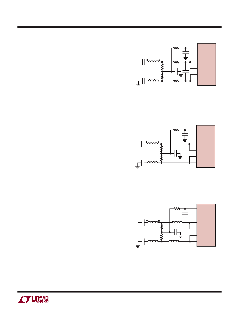
For input frequencies above 100MHz the input circuits of
Figure 6, 7 and 8 are recommended. The balun transformer
gives better high frequency response than a ux coupled
center tapped transformer. The coupling capacitors allow
the analog inputs to be DC biased at 1.25V. In Figure 8 the
series inductors are impedance matching elements that
maximize the ADC bandwidth.
Reference Operation
Figure 9 shows the LTC2240-10 reference circuitry consist-
ing of a 1.25V bandgap reference, a difference amplier
and switching and control circuit. The internal voltage
reference can be congured for two pin selectable input
ranges of 2V (±1V differential) or 1V (±0.5V differential).
Tying the SENSE pin to VDD selects the 2V range; typing
the SENSE pin to VCM selects the 1V range.
The 1.25V bandgap reference serves two functions: its
output provides a DC bias point for setting the common
mode voltage of any external input circuitry; additionally,
the reference is used with a difference amplier to gener-
ate the differential reference levels needed by the internal
ADC circuitry. An external bypass capacitor is required
for the 1.25V reference output, VCM. This provides a high
frequency low impedance path to ground for internal and
external circuitry.
The difference amplier generates the high and low
reference for the ADC. High speed switching circuits are
connected to these outputs and they must be externally
bypassed. Each output has four pins: two each of REFHA
and REFHB for the high reference and two each of REFLA
and REFLB for the low reference. The multiple output pins
are needed to reduce package inductance. Bypass capaci-
tors must be connected as shown in Figure 9.
Figure 6. Recommended Front End Circuit for
Input Frequencies Between 100MHz and 250MHz
Figure 7. Recommended Front End Circuit for
Input Frequencies Between 250MHz and 500MHz
Figure 8. Recommended Front End Circuit for
Input Frequencies Above 500MHz
25Ω
12Ω
10Ω
0.1μF
AIN
+
AIN
+
AIN
–
AIN
–
8pF
2.2μF
VCM
ANALOG
INPUT
0.1μF
T1
T1 = MA/COM ETC1-1-13
RESISTORS, CAPACITORS
ARE 0402 PACKAGE SIZE
224010 F06
LTC2240-10
25Ω
10Ω
25Ω
0.1μF
AIN
+
AIN
+
AIN
–
AIN
–
2.2μF
VCM
ANALOG
INPUT
0.1μF
T1
T1 = MA/COM ETC1-1-13
RESISTORS, CAPACITORS
ARE 0402 PACKAGE SIZE
224010 F07
LTC2240-10
25Ω
10Ω
25Ω
0.1μF
AIN
+
AIN
+
AIN
–
AIN
–
2.2μF
VCM
LTC2240-10
ANALOG
INPUT
0.1μF
T1
T1 = MA/COM ETC1-1-13
RESISTORS, CAPACITORS
ARE 0402 PACKAGE SIZE
224010 F08
2.7nH
相关PDF资料 |
PDF描述 |
|---|---|
| MS27497E16F35S | CONN RCPT 55POS WALL MNT W/SCKT |
| IDT72V05L35J8 | IC FIFO ASYNCH 4096X18 32PLCC |
| AD7892AN-2 | IC ADC 12BIT LP 500KSPS 24-DIP |
| ADM207AN | IC TXRX RS232 5DVR/3REC 24DIP |
| IDT72V211L20PF | IC FIFO SYNC 512X9 20NS 32-TQFP |
相关代理商/技术参数 |
参数描述 |
|---|---|
| LTC2240CUP-12 | 制造商:LINER 制造商全称:Linear Technology 功能描述:12-Bit, 170Msps ADC |
| LTC2240CUP-12#PBF | 功能描述:IC ADC 12BIT 170MSPS 64-QFN RoHS:是 类别:集成电路 (IC) >> 数据采集 - 模数转换器 系列:- 标准包装:1 系列:- 位数:14 采样率(每秒):83k 数据接口:串行,并联 转换器数目:1 功率耗散(最大):95mW 电压电源:双 ± 工作温度:0°C ~ 70°C 安装类型:通孔 封装/外壳:28-DIP(0.600",15.24mm) 供应商设备封装:28-PDIP 包装:管件 输入数目和类型:1 个单端,双极 |
| LTC2240CUP-12#TRPBF | 功能描述:IC ADC 12BIT 170MSPS 64-QFN RoHS:是 类别:集成电路 (IC) >> 数据采集 - 模数转换器 系列:- 标准包装:1 系列:- 位数:14 采样率(每秒):83k 数据接口:串行,并联 转换器数目:1 功率耗散(最大):95mW 电压电源:双 ± 工作温度:0°C ~ 70°C 安装类型:通孔 封装/外壳:28-DIP(0.600",15.24mm) 供应商设备封装:28-PDIP 包装:管件 输入数目和类型:1 个单端,双极 |
| LTC2240CUP-12-PBF | 制造商:LINER 制造商全称:Linear Technology 功能描述:12-Bit, 170Msps ADC |
| LTC2240CUP-12-TR | 制造商:LINER 制造商全称:Linear Technology 功能描述:12-Bit, 170Msps ADC |
发布紧急采购,3分钟左右您将得到回复。