- 您现在的位置:买卖IC网 > PDF目录2005 > LTC2262CUJ-14#TRPBF (Linear Technology)IC ADC 14BIT 150MSPS 40-QFN PDF资料下载
参数资料
| 型号: | LTC2262CUJ-14#TRPBF |
| 厂商: | Linear Technology |
| 文件页数: | 11/28页 |
| 文件大小: | 0K |
| 描述: | IC ADC 14BIT 150MSPS 40-QFN |
| 标准包装: | 2,000 |
| 位数: | 14 |
| 采样率(每秒): | 150M |
| 数据接口: | 并联 |
| 转换器数目: | 1 |
| 功率耗散(最大): | 171mW |
| 电压电源: | 单电源 |
| 工作温度: | 0°C ~ 70°C |
| 安装类型: | 表面贴装 |
| 封装/外壳: | 40-WFQFN 裸露焊盘 |
| 供应商设备封装: | 40-QFN(6x6) |
| 包装: | 带卷 (TR) |
| 输入数目和类型: | 1 个差分 |
| 配用: | DC890B-ND - BOARD USB DATA COLLECTION |
第1页第2页第3页第4页第5页第6页第7页第8页第9页第10页当前第11页第12页第13页第14页第15页第16页第17页第18页第19页第20页第21页第22页第23页第24页第25页第26页第27页第28页
19
226214fc
LTC2262-14
For more information www.linear.com/LTC2262-14
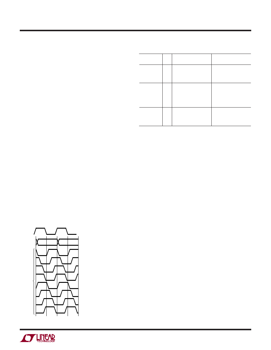
Phase Shifting the Output Clock
In full-rate CMOS mode the data output bits normally
change at the same time as the falling edge of CLKOUT+,
so the rising edge of CLKOUT+ can be used to latch the
output data. In double data rate CMOS and LVDS modes
the data output bits normally change at the same time as
the falling and rising edges of CLKOUT+. To allow adequate
setup-and-hold time when latching the data, the CLKOUT+
signal may need to be phase shifted relative to the data
output bits. Most FPGAs have this feature; this is generally
the best place to adjust the timing.
The LTC2262-14 can also phase shift the CLKOUT+/
CLKOUT– signals by serially programming mode con-
trol register A2. The output clock can be shifted by
0°, 45°, 90° or 135°. To use the phase shifting feature
the clock duty cycle stabilizer must be turned on.
Another control register bit can invert the polarity of
CLKOUT+ and CLKOUT–, independently of the phase shift.
The combination of these two features enables phase
shifts of 45° up to 315° (Figure 14).
DATA FORMAT
Table 1 shows the relationship between the analog input
voltage, the digital data output bits and the overflow bit.
By default the output data format is offset binary. The 2’s
complement format can be selected by serially program-
ming mode control register A4
Table 1. Output Codes vs Input Voltage
AIN+ – AIN–
(2V Range)
OF
D13-D0
(OFFSET BINARY)
D13-D0
(2’s COMPLEMENT)
>1.000000V
+0.999878V
+0.999756V
1
0
11 1111 1111 1111
11 1111 1111 1110
01 1111 1111 1111
01 1111 1111 1110
+0.000122V
+0.000000V
–0.000122V
–0.000244V
0
10 0000 0000 0001
10 0000 0000 0000
01 1111 1111 1111
01 1111 1111 1110
00 0000 0000 0001
00 0000 0000 0000
11 1111 1111 1111
11 1111 1111 1110
–0.999878V
–1.000000V
≤–1.000000V
0
1
00 0000 0000 0001
00 0000 0000 0000
10 0000 0000 0001
10 0000 0000 0000
Digital Output Randomizer
Interference from the A/D digital outputs is sometimes
unavoidable.Digitalinterferencemaybefromcapacitiveor
inductive coupling or coupling through the ground plane.
Even a tiny coupling factor can cause unwanted tones
in the ADC output spectrum. By randomizing the digital
output before it is transmitted off chip, these unwanted
tones can be randomized which reduces the unwanted
tone amplitude.
The digital output is “randomized” by applying an exclu-
sive-OR logic operation between the LSB and all other
data output bits. To decode, the reverse operation is ap-
plied—an exclusive-OR operation is applied between the
LSB and all other bits. The LSB, OF and CLKOUT outputs
are not affected. The output randomizer is enabled by
serially programming mode control register A4.
Alternate Bit Polarity
Another feature that reduces digital feedback on the circuit
board is the alternate bit polarity mode. When this mode
is enabled, all of the odd bits (D1, D3, D5, D7, D9, D11,
D13) are inverted before the output buffers. The even bits
(D0, D2, D4, D6, D8, D10, D12), OF and CLKOUT are not
affected. This can reduce digital currents in the circuit
board ground plane and reduce digital noise, particularly
for very small analog input signals.
When there is a very small signal at the input of the A/D
thatiscenteredaroundmidscale,thedigitaloutputstoggle
between mostly 1s and mostly 0s. This simultaneous
APPLICATIONS INFORMATION
Figure 14. Phase Shifting CLKOUT
CLKOUT+
D0-D13, OF
PHASE
SHIFT
0°
45°
90°
135°
180°
225°
270°
315°
CLKINV
0
1
CLKPHASE1
MODE CONTROL BITS
0
1
0
1
CLKPHASE0
0
1
0
1
0
1
0
1
226214 F14
ENC+
相关PDF资料 |
PDF描述 |
|---|---|
| LTC2262IUJ-12#PBF | IC ADC 12BIT 150MSPS 40-QFN |
| LTC2264CUJ-12#PBF | IC ADC 12BIT SER/PAR 40M 40-QFN |
| LTC2268IUJ-14#TRPBF | IC ADC 14BIT 125MSPS DUAL 40QFN |
| LTC2280CUP#PBF | IC ADC DUAL 10BIT 105MSPS 64-QFN |
| LTC2281IUP#PBF | IC ADC 10BIT DUAL 64-QFN |
相关代理商/技术参数 |
参数描述 |
|---|---|
| LTC2262IUJ-12#PBF | 功能描述:IC ADC 12BIT 150MSPS 40-QFN RoHS:是 类别:集成电路 (IC) >> 数据采集 - 模数转换器 系列:- 标准包装:1 系列:- 位数:14 采样率(每秒):83k 数据接口:串行,并联 转换器数目:1 功率耗散(最大):95mW 电压电源:双 ± 工作温度:0°C ~ 70°C 安装类型:通孔 封装/外壳:28-DIP(0.600",15.24mm) 供应商设备封装:28-PDIP 包装:管件 输入数目和类型:1 个单端,双极 |
| LTC2262IUJ-12#TRPBF | 功能描述:IC ADC 12BIT 150MSPS 40-QFN RoHS:是 类别:集成电路 (IC) >> 数据采集 - 模数转换器 系列:- 标准包装:1 系列:- 位数:14 采样率(每秒):83k 数据接口:串行,并联 转换器数目:1 功率耗散(最大):95mW 电压电源:双 ± 工作温度:0°C ~ 70°C 安装类型:通孔 封装/外壳:28-DIP(0.600",15.24mm) 供应商设备封装:28-PDIP 包装:管件 输入数目和类型:1 个单端,双极 |
| LTC2262IUJ-14#PBF | 制造商:Linear Technology 功能描述:ADC Single Pipelined 150Msps 14-bit Parallel/LVDS 40-Pin QFN EP 制造商:Linear Technology 功能描述:IC ADC 14BIT 1.8V 150MSPS 40-QFN |
| LTC2262IUJ-14#TRPBF | 制造商:Linear Technology 功能描述:ADC Single Pipelined 150Msps 14-bit Parallel/LVDS 40-Pin QFN EP T/R 制造商:Linear Technology 功能描述:IC ADC 14BIT 150MSPS 40-QFN |
| LTC2263-12 | 制造商:LINER 制造商全称:Linear Technology 功能描述:12-Bit, 65Msps/40Msps/25Msps Low Power Dual ADCs |
发布紧急采购,3分钟左右您将得到回复。