- 您现在的位置:买卖IC网 > PDF目录39416 > LTC2263IUJ-14#PBF (LINEAR TECHNOLOGY CORP) PROPRIETARY METHOD ADC, QCC40 PDF资料下载
参数资料
| 型号: | LTC2263IUJ-14#PBF |
| 厂商: | LINEAR TECHNOLOGY CORP |
| 元件分类: | ADC |
| 英文描述: | PROPRIETARY METHOD ADC, QCC40 |
| 封装: | 6 X 6 MM, LEAD FREE, PLASTIC, QFN-40 |
| 文件页数: | 14/32页 |
| 文件大小: | 1451K |
| 代理商: | LTC2263IUJ-14#PBF |
第1页第2页第3页第4页第5页第6页第7页第8页第9页第10页第11页第12页第13页当前第14页第15页第16页第17页第18页第19页第20页第21页第22页第23页第24页第25页第26页第27页第28页第29页第30页第31页第32页
LTC2265-14/
LTC2264-14/LTC2263-14
21
22654314fb
APPLICATIONS INFORMATION
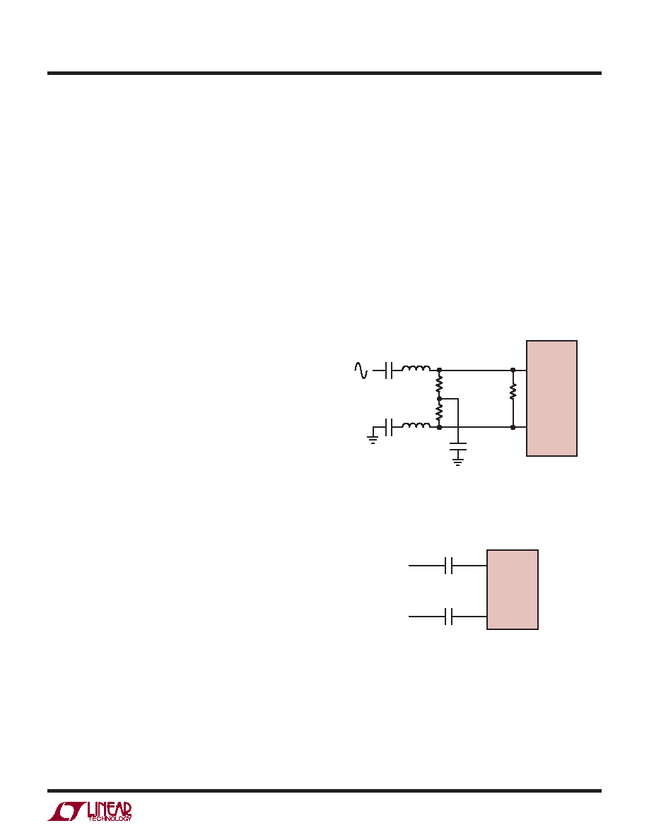
The differential encode mode is recommended for sinu-
soidal, PECL, or LVDS encode inputs (Figures 12 and 13).
The encode inputs are internally biased to 1.2V through
10k equivalent resistance. The encode inputs can be taken
above VDD (up to 3.6V), and the common mode range
is from 1.1V to 1.6V. In the differential encode mode,
ENC– should stay at least 200mV above ground to avoid
falsely triggering the single-ended encode mode. For
good jitter performance ENC+ should have fast rise and
fall times.
The single-ended encode mode should be used with
CMOS encode inputs. To select this mode, ENC– is con-
nected to ground and ENC+ is driven with a square wave
encode input. ENC+ can be taken above VDD (up to 3.6V)
so 1.8V to 3.3V CMOS logic levels can be used. The
ENC+ threshold is 0.9V. For good jitter performance
ENC+ should have fast rise and fall times.
Clock PLL and Duty Cycle Stabilizer
The encode clock is multiplied by an internal phase-locked
loop (PLL) to generate the serial digital output data. If the
encode signal changes frequency or is turned off, the PLL
requires 25s to lock onto the input clock.
A clock duty cycle stabilizer circuit allows the duty cycle
of the applied encode signal to vary from 30% to 70%.
In the serial programming mode it is possible to disable
the duty cycle stabilizer, but this is not recommended. In
the parallel programming mode the duty cycle stabilizer
is always enabled.
DIGITAL OUTPUTS
The digital outputs of the LTC2265-14/LTC2264-14/
LTC2263-14 are serialized LVDS signals. Each channel
outputs two bits at a time (2-lane mode) or one bit at a time
(1-lane mode). The data can be serialized with 16-, 14-, or
12-bit serialization (see the Timing Diagrams section for
details). Note that with 12-bit serialization the two LSBs
are not available—this mode is included for compatibility
with the 12-bit versions of these parts.
The output data should be latched on the rising and falling
edges of the data clockout (DCO). A data frame output
(FR) can be used to determine when the data from a new
conversion result begins. In the 2-lane, 14-bit serialization
mode, the frequency of the FR output is halved.
The maximum serial data rate for the data outputs is
1Gbps, so the maximum sample rate of the ADC will de-
pend on the serialization mode as well as the speed grade
of the ADC (see Table 1). The minimum sample rate for
all serialization modes is 5Msps.
50
100
0.1F
T1
T1 = MA/COM ETC1-1-13
RESISTORS AND CAPACITORS
ARE 0402 PACKAGE SIZE
50
LTC2265-14
226514 F12
ENC–
ENC+
ENC+
ENC–
PECL OR
LVDS
CLOCK
0.1F
226514 F13
LTC2265-14
Figure 12. Sinusoidal Encode Drive
Figure 13. PECL or LVDS Encode Drive
相关PDF资料 |
PDF描述 |
|---|---|
| LTC2264CUJ-14#PBF | PROPRIETARY METHOD ADC, QCC40 |
| LTC2265CUJ-14#TRPBF | PROPRIETARY METHOD ADC, QCC40 |
| LTC2265IUJ-14#PBF | PROPRIETARY METHOD ADC, QCC40 |
| LTC2265IUJ-12#PBF | PROPRIETARY METHOD ADC, QCC40 |
| LTC2265CUJ-12#TRPBF | PROPRIETARY METHOD ADC, QCC40 |
相关代理商/技术参数 |
参数描述 |
|---|---|
| LTC2263IUJ-14TRPBF | 制造商:LINER 制造商全称:Linear Technology 功能描述:14-Bit, 65Msps/40Msps/25Msps Low Power Dual ADCs |
| LTC2264-12 | 制造商:LINER 制造商全称:Linear Technology 功能描述:12-Bit, 65Msps/40Msps/25Msps Low Power Dual ADCs |
| LTC2264-14 | 制造商:LINER 制造商全称:Linear Technology 功能描述:Quad 14-Bit, 125Msps ADC with Integrated Drivers |
| LTC2264CUJ-12#PBF | 功能描述:IC ADC 12BIT SER/PAR 40M 40-QFN RoHS:是 类别:集成电路 (IC) >> 数据采集 - 模数转换器 系列:- 标准包装:1 系列:- 位数:14 采样率(每秒):83k 数据接口:串行,并联 转换器数目:1 功率耗散(最大):95mW 电压电源:双 ± 工作温度:0°C ~ 70°C 安装类型:通孔 封装/外壳:28-DIP(0.600",15.24mm) 供应商设备封装:28-PDIP 包装:管件 输入数目和类型:1 个单端,双极 |
| LTC2264CUJ-12#TRPBF | 功能描述:IC ADC 12BIT SER/PAR 40M 40-QFN RoHS:是 类别:集成电路 (IC) >> 数据采集 - 模数转换器 系列:- 标准包装:1,000 系列:- 位数:12 采样率(每秒):300k 数据接口:并联 转换器数目:1 功率耗散(最大):75mW 电压电源:单电源 工作温度:0°C ~ 70°C 安装类型:表面贴装 封装/外壳:24-SOIC(0.295",7.50mm 宽) 供应商设备封装:24-SOIC 包装:带卷 (TR) 输入数目和类型:1 个单端,单极;1 个单端,双极 |
发布紧急采购,3分钟左右您将得到回复。