- 您现在的位置:买卖IC网 > PDF目录10212 > LTC2280CUP#TRPBF (Linear Technology)IC ADC DUAL 10BIT 105MSPS 64-QFN PDF资料下载
参数资料
| 型号: | LTC2280CUP#TRPBF |
| 厂商: | Linear Technology |
| 文件页数: | 24/24页 |
| 文件大小: | 0K |
| 描述: | IC ADC DUAL 10BIT 105MSPS 64-QFN |
| 标准包装: | 2,000 |
| 位数: | 10 |
| 采样率(每秒): | 105M |
| 数据接口: | 并联 |
| 转换器数目: | 2 |
| 功率耗散(最大): | 630mW |
| 电压电源: | 单电源 |
| 工作温度: | 0°C ~ 70°C |
| 安装类型: | 表面贴装 |
| 封装/外壳: | 64-WFQFN 裸露焊盘 |
| 供应商设备封装: | 64-QFN(9x9) |
| 包装: | 带卷 (TR) |
| 输入数目和类型: | 2 个单端,双极; 2 个差分, 双极 |
LTC2280
9
2280fa
SHIFT REGISTER
AND CORRECTION
DIFF
REF
AMP
REF
BUF
2.2
F
1
F1F
0.1
F
INTERNAL CLOCK SIGNALS
REFH
REFL
CLOCK/DUTY
CYCLE
CONTROL
RANGE
SELECT
1.5V
REFERENCE
FIRST PIPELINED
ADC STAGE
FIFTH PIPELINED
ADC STAGE
SIXTH PIPELINED
ADC STAGE
FOURTH PIPELINED
ADC STAGE
SECOND PIPELINED
ADC STAGE
REFH
REFL
CLK
OE
MODE
OGND
OVDD
2280 F01
INPUT
S/H
SENSE
VCM
AIN
–
AIN
+
2.2
F
THIRD PIPELINED
ADC STAGE
OUTPUT
DRIVERS
CONTROL
LOGIC
SHDN
OF
D9
D0
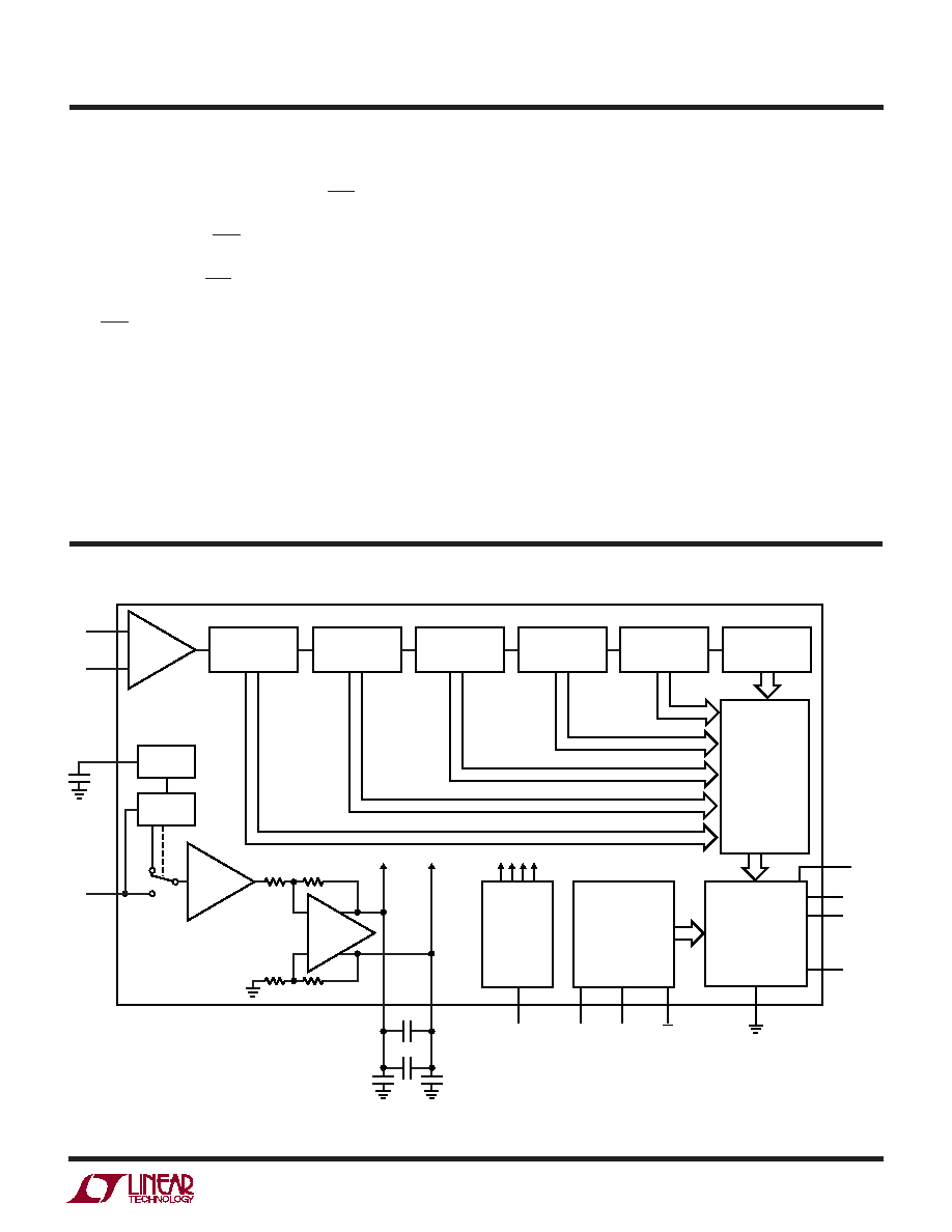
SHDNA (Pin 59): Channel A Shutdown Mode Selection
Pin. Connecting SHDNA to GND and OEA to GND results
in normal operation with the outputs enabled. Connecting
SHDNA to GND and OEA to VDD results in normal opera-
tion with the outputs at high impedance. Connecting
SHDNA to VDD and OEA to GND results in nap mode with
the outputs at high impedance. Connecting SHDNA to VDD
and OEA to VDD results in sleep mode with the outputs at
high impedance.
MODE (Pin 60): Output Format and Clock Duty Cycle
Stabilizer Selection Pin. Note that MODE controls both
channels. Connecting MODE to GND selects offset binary
output format and turns the clock duty cycle stabilizer off.
1/3 VDD selects offset binary output format and turns the
clock duty cycle stabilizer on. 2/3 VDD selects 2’s comple-
ment output format and turns the clock duty cycle
UU
U
PI FU CTIO S
stabilizer on. VDD selects 2’s complement output format
and turns the clock duty cycle stabilizer off.
VCMA (Pin 61): Channel A 1.5V Output and Input Common
Mode Bias. Bypass to ground with 2.2
F ceramic chip
capacitor. Do not connect to VCMB.
SENSEA (Pin 62): Channel A Reference Programming Pin.
Connecting SENSEA to VCMA selects the internal reference
and a
±0.5V input range. VDD selects the internal reference
and a
±1V input range. An external reference greater than
0.5V and less than 1V applied to SENSEA selects an input
range of
±VSENSEA. ±1V is the largest valid input range.
GND (Exposed Pad) (Pin 65): ADC Power Ground. The
Exposed Pad on the bottom of the package needs to be
soldered to ground.
FUNCTIONAL BLOCK DIAGRA
UU
W
Figure 1. Functional Block Diagram (Only One Channel is Shown)
相关PDF资料 |
PDF描述 |
|---|---|
| SP3084EEN-L/TR | IC TXRX RS485/RS422 ESD 8NSOIC |
| AD7357BRUZ-RL | IC ADC 14BITDUAL 4.MSPS 16TSSOP |
| SP3083EEN-L/TR | IC TXRX RS485/RS422 ESD 14NSOIC |
| SP3081EEN-L/TR | IC TXRX RS485/RS422 ESD 8NSOIC |
| SP3080EEN-L/TR | IC TXRX RS485/RS422 ESD 14NSOIC |
相关代理商/技术参数 |
参数描述 |
|---|---|
| LTC2280IUP | 制造商:LINER 制造商全称:Linear Technology 功能描述:Dual 10-Bit, 105Msps Low Noise 3V ADC |
| LTC2280IUP#PBF | 功能描述:IC ADC DUAL 10BIT 105MSPS 64-QFN RoHS:是 类别:集成电路 (IC) >> 数据采集 - 模数转换器 系列:- 其它有关文件:TSA1204 View All Specifications 标准包装:1 系列:- 位数:12 采样率(每秒):20M 数据接口:并联 转换器数目:2 功率耗散(最大):155mW 电压电源:模拟和数字 工作温度:-40°C ~ 85°C 安装类型:表面贴装 封装/外壳:48-TQFP 供应商设备封装:48-TQFP(7x7) 包装:Digi-Reel® 输入数目和类型:4 个单端,单极;2 个差分,单极 产品目录页面:1156 (CN2011-ZH PDF) 其它名称:497-5435-6 |
| LTC2280IUP#TRPBF | 功能描述:IC ADC DUAL 10BIT 105MSPS 64-QFN RoHS:是 类别:集成电路 (IC) >> 数据采集 - 模数转换器 系列:- 标准包装:1,000 系列:- 位数:12 采样率(每秒):300k 数据接口:并联 转换器数目:1 功率耗散(最大):75mW 电压电源:单电源 工作温度:0°C ~ 70°C 安装类型:表面贴装 封装/外壳:24-SOIC(0.295",7.50mm 宽) 供应商设备封装:24-SOIC 包装:带卷 (TR) 输入数目和类型:1 个单端,单极;1 个单端,双极 |
| LTC2280UP | 制造商:LINER 制造商全称:Linear Technology 功能描述:Dual 10-Bit, 105Msps Low Noise 3V ADC |
| LTC2281 | 制造商:LINER 制造商全称:Linear Technology 功能描述:Dual 10-Bit, 125Msps Low Power 3V ADC |
发布紧急采购,3分钟左右您将得到回复。