- 您现在的位置:买卖IC网 > PDF目录10073 > LTC2282CUP#TRPBF (Linear Technology)IC ADC DUAL 12BIT 105MSPS 64-QFN PDF资料下载
参数资料
| 型号: | LTC2282CUP#TRPBF |
| 厂商: | Linear Technology |
| 文件页数: | 10/24页 |
| 文件大小: | 0K |
| 描述: | IC ADC DUAL 12BIT 105MSPS 64-QFN |
| 标准包装: | 2,000 |
| 位数: | 12 |
| 采样率(每秒): | 105M |
| 数据接口: | 并联 |
| 转换器数目: | 2 |
| 功率耗散(最大): | 630mW |
| 电压电源: | 单电源 |
| 工作温度: | 0°C ~ 70°C |
| 安装类型: | 表面贴装 |
| 封装/外壳: | 64-WFQFN 裸露焊盘 |
| 供应商设备封装: | 64-QFN(9x9) |
| 包装: | 带卷 (TR) |
| 输入数目和类型: | 2 个单端,双极; 2 个差分, 双极 |
LTC2282
18
2282fb
APPLICATIONS INFORMATION
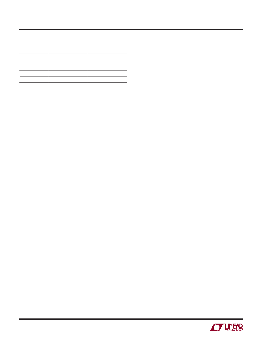
Table 2. MODE Pin Function
MODE Pin
Output Format
Clock Duty
Cycle Stabilizer
0
Offset Binary
Off
1/3VDD
Offset Binary
On
2/3VDD
2’s Complement
On
VDD
2’s Complement
Off
Overow Bit
When OF outputs a logic high the converter is either over-
ranged or underranged.
Output Driver Power
Separate output power and ground pins allow the output
drivers to be isolated from the analog circuitry. The power
supplyforthedigitaloutputbuffers,OVDD,shouldbetiedtothe
samepowersupplyasforthelogicbeingdriven.Forexample,
if the converter is driving a DSP powered by a 1.8V supply,
then OVDD should be tied to that same 1.8V supply.
OVDD can be powered with any voltage from 500mV up to
3.6V. OGND can be powered with any voltage from GND
up to 1V and must be less than OVDD. The logic outputs
will swing between OGND and OVDD.
Output Enable
The outputs may be disabled with the output enable pin,
OE. OE high disables all data outputs including OF. The
data access and bus relinquish times are too slow to
allow the outputs to be enabled and disabled during full
speed operation. The output Hi-Z state is intended for use
during long periods of inactivity. Channels A and B have
independent output enable pins (OEA, OEB).
Sleep and Nap Modes
The converter may be placed in shutdown or nap modes
to conserve power. Connecting SHDN to GND results in
normal operation. Connecting SHDN to VDD and OE to VDD
results in sleep mode, which powers down all circuitry,
including the reference, and typically dissipates 1mW.
When exiting sleep mode, it will take milliseconds for the
output data to become valid because the reference capaci-
tors have to recharge and stabilize. Connecting SHDN to
VDD and OE to GND results in nap mode, which typically
dissipates 30mW. In nap mode, the on-chip reference circuit
is kept on, so that recovery from nap mode is faster than
that from sleep mode, typically taking 100 clock cycles. In
both sleep and nap modes, all digital outputs are disabled
and enter the Hi-Z state.
Channels A and B have independent SHDN pins (SHDNA,
SHDNB). Channel A is controlled by SHDNA and OEA, and
channel B is controlled by SHDNB and OEB. The nap, sleep
andoutputenablemodesofthetwochannelsarecompletely
independent, so it is possible to have one channel operating
while the other channel is in nap or sleep mode.
Digital Output Multiplexer
The digital outputs of the LTC2282 can be multiplexed onto
a single data bus if the sample rate is 80Msps, or less. The
MUX pin is a digital input that swaps the two data busses.
If MUX is high, channel A comes out on DA0-DA11, OFA;
channel B comes out on DB0-DB11, OFB. If MUX is low,
the output busses are swapped and channel A comes out
on DB0-DB11, OFB; channel B comes out on DA0-DA11,
OFA. To multiplex both channels onto a single output bus,
connect MUX, CLKA and CLKB together (see the Timing
Diagram for the multiplexed mode). The multiplexed data
is available on either data bus—the unused data bus can
be disabled with its OE pin.
Grounding and Bypassing
The LTC2282 requires a printed circuit board with a clean,
unbroken ground plane. A multilayer board with an internal
ground plane is recommended. Layout for the printed
circuit board should ensure that digital and analog signal
lines are separated as much as possible. In particular, care
should be taken not to run any digital track alongside an
analog signal track or underneath the ADC.
相关PDF资料 |
PDF描述 |
|---|---|
| VE-BN1-IV-F4 | CONVERTER MOD DC/DC 12V 150W |
| LTC2262CUJ-12#TRPBF | IC ADC 12BIT 150MSPS 40-QFN |
| MS27473E18B11P | CONN PLUG 11POS STRAIGHT W/PINS |
| AD7876CR-REEL | IC ADC 12BIT SAMPLING 10V 24SOIC |
| AD976ABRZRL | IC ADC 16BIT 200KSPS 28SOIC |
相关代理商/技术参数 |
参数描述 |
|---|---|
| LTC2282IUP | 制造商:Linear Technology 功能描述:ADC Dual Pipelined 105Msps 12-bit Parallel 64-Pin QFN EP |
| LTC2282IUP#PBF | 功能描述:IC ADC DUAL 12BIT 105MSPS 64-QFN RoHS:是 类别:集成电路 (IC) >> 数据采集 - 模数转换器 系列:- 标准包装:1 系列:microPOWER™ 位数:8 采样率(每秒):1M 数据接口:串行,SPI? 转换器数目:1 功率耗散(最大):- 电压电源:模拟和数字 工作温度:-40°C ~ 125°C 安装类型:表面贴装 封装/外壳:24-VFQFN 裸露焊盘 供应商设备封装:24-VQFN 裸露焊盘(4x4) 包装:Digi-Reel® 输入数目和类型:8 个单端,单极 产品目录页面:892 (CN2011-ZH PDF) 其它名称:296-25851-6 |
| LTC2282IUP#TRPBF | 功能描述:IC ADC DUAL 12BIT 105MSPS 64-QFN RoHS:是 类别:集成电路 (IC) >> 数据采集 - 模数转换器 系列:- 标准包装:1 系列:- 位数:14 采样率(每秒):83k 数据接口:串行,并联 转换器数目:1 功率耗散(最大):95mW 电压电源:双 ± 工作温度:0°C ~ 70°C 安装类型:通孔 封装/外壳:28-DIP(0.600",15.24mm) 供应商设备封装:28-PDIP 包装:管件 输入数目和类型:1 个单端,双极 |
| LTC2282IUP-PBF | 制造商:LINER 制造商全称:Linear Technology 功能描述:Dual 12-Bit, 105Msps Low Power 3V ADC |
| LTC2282IUP-TR | 制造商:LINER 制造商全称:Linear Technology 功能描述:Dual 12-Bit, 105Msps Low Power 3V ADC |
发布紧急采购,3分钟左右您将得到回复。