- 您现在的位置:买卖IC网 > PDF目录39417 > LTC2356IMSE-12#TR (LINEAR TECHNOLOGY CORP) 1-CH 12-BIT PROPRIETARY METHOD ADC, SERIAL ACCESS, PDSO10 PDF资料下载
参数资料
| 型号: | LTC2356IMSE-12#TR |
| 厂商: | LINEAR TECHNOLOGY CORP |
| 元件分类: | ADC |
| 英文描述: | 1-CH 12-BIT PROPRIETARY METHOD ADC, SERIAL ACCESS, PDSO10 |
| 封装: | PLASTIC, MSOP-10 |
| 文件页数: | 5/16页 |
| 文件大小: | 266K |
| 代理商: | LTC2356IMSE-12#TR |
13
LTC2356-12/LTC2356-14
2356f
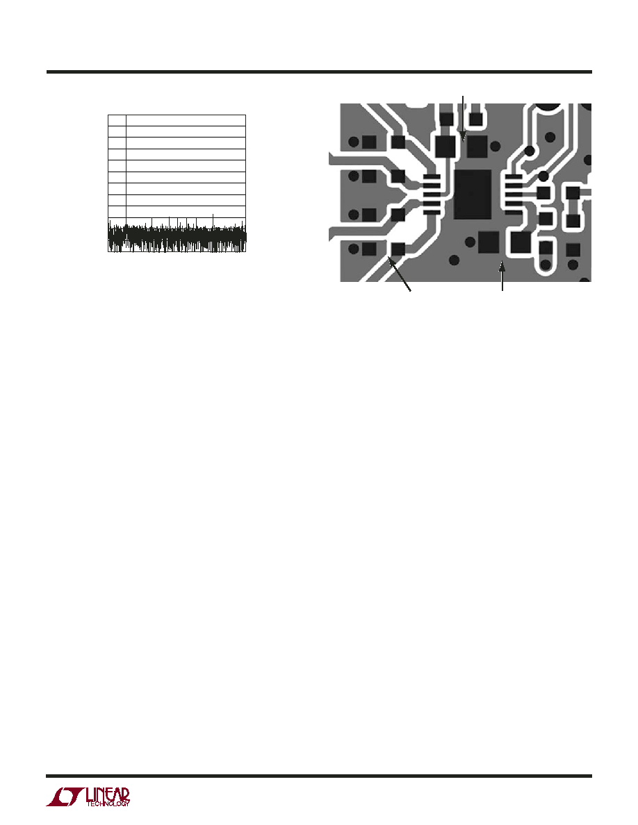
Board Layout and Bypassing
Wire wrap boards are not recommended for high resolu-
tion and/or high speed A/D converters. To obtain the best
performance from the LTC2356-12/LTC2356-14, a printed
circuit board with ground plane is required. Layout for the
printed circuit board should ensure that digital and analog
signal lines are separated as much as possible. In particu-
lar, care should be taken not to run any digital track
alongside an analog signal track. If optimum phase match
between the inputs is desired, the length of the two input
wires should be kept matched.
High quality tantalum and ceramic bypass capacitors
should be used at the VDD and VREF pins as shown in the
Block Diagram on the first page of this data sheet. For
optimum performance, a 10
F surface mount Tantalum
capacitor with a 0.1
F ceramic is recommended for the
VDD and VREF pins. Alternatively, 10F ceramic chip
capacitors such as Murata GRM219R60J106M may
be used. The capacitors must be located as close to the
pins as possible. The traces connecting the pins and the
bypass capacitors must be kept short and should be made
as wide as possible.
Figure 7 shows the recommended system ground connec-
tions. All analog circuitry grounds should be terminated at
the LTC2356-12/LTC2356-14 GND (Pins 4, 5, 6 and
exposed pad). The ground return from the LTC2356-12/
LTC2356-14 (Pins 4, 5, 6 and exposed pad) to the power
supply should be low impedance for noise free operation.
In applications where the ADC data outputs and control
signals are connected to a continuously active micropro-
cessor bus, it is possible to get errors in the conversion
results. These errors are due to feedthrough from the
microprocessor to the successive approximation com-
parator. The problem can be eliminated by forcing the
microprocessor into a Wait state during conversion or by
using three-state buffers to isolate the ADC data bus.
POWER-DOWN MODES
Upon power-up, the LTC2356-12/LTC2356-14 is initial-
ized to the active state and is ready for conversion. The Nap
and Sleep mode waveforms show the power-down modes
for the LTC2356-12/LTC2356-14. The SCK and CONV
inputs control the power-down modes (see Timing
Diagrams). Two rising edges at CONV, without any
intervening rising edges at SCK, put the LTC2356-12/
LTC2356-14 in Nap mode and the power consumption
drops from 18mW to 4mW. The internal reference
remains powered in Nap mode. One or more rising edges
at SCK wake up the LTC2356-12/LTC2356-14 very quickly,
and CONV can start an accurate conversion within a clock
cycle. Four rising edges at CONV, without any intervening
rising edges at SCK, put the LTC2356-12/LTC2356-14 in
Sleep mode and the power consumption drops from
18mW to 13
W. One or more rising edges at SCK wake up
the LTC2356-12/LTC2356-14 for operation. The internal
reference (VREF ) takes 2ms to slew and settle with a 10F
load. Note that, using sleep mode more frequently than
every 2ms, compromises the settled accuracy of the
APPLICATIO S I FOR ATIO
WU
U
Figure 7. Recommended Layout
2356 F07
FREQUENCY (Hz)
MAGNITUDE
(dB)
–60
–30
–20
2356 F06b
–70
–80
–120
–100
0
–10
–40
–50
–90
–110
0
371k
185k
556k
741k
Figure 6b. LTC2356-12 6MHz Sine Wave 4096 Point FFT Plot
with the LT1819 Driving the Inputs Differentially
VREF BYPASS 0805 SIZE
VDD BYPASS 0805 SIZE
OPTIONAL INPUT FILTERING
相关PDF资料 |
PDF描述 |
|---|---|
| LTC2356IMSE-14#TR | 1-CH 14-BIT PROPRIETARY METHOD ADC, SERIAL ACCESS, PDSO10 |
| LTC2356CMSE-14#TR | 1-CH 14-BIT PROPRIETARY METHOD ADC, SERIAL ACCESS, PDSO10 |
| LTC2356CMSE-14#TRPBF | 1-CH 14-BIT PROPRIETARY METHOD ADC, SERIAL ACCESS, PDSO10 |
| LTC2356IMSE-14#TRPBF | 1-CH 14-BIT PROPRIETARY METHOD ADC, SERIAL ACCESS, PDSO10 |
| LTC2376CDE-16#PBF | 1-CH 16-BIT SUCCESSIVE APPROXIMATION ADC, SERIAL ACCESS, PDSO16 |
相关代理商/技术参数 |
参数描述 |
|---|---|
| LTC2356IMSE-14 | 制造商:Linear Technology 功能描述:IC ADC 14BIT 3 WIRE SPI 3.5MSPS |
| LTC2356IMSE-14#PBF | 功能描述:IC ADC 14BIT 3.5MSPS 10-MSOP RoHS:是 类别:集成电路 (IC) >> 数据采集 - 模数转换器 系列:- 标准包装:1 系列:microPOWER™ 位数:8 采样率(每秒):1M 数据接口:串行,SPI? 转换器数目:1 功率耗散(最大):- 电压电源:模拟和数字 工作温度:-40°C ~ 125°C 安装类型:表面贴装 封装/外壳:24-VFQFN 裸露焊盘 供应商设备封装:24-VQFN 裸露焊盘(4x4) 包装:Digi-Reel® 输入数目和类型:8 个单端,单极 产品目录页面:892 (CN2011-ZH PDF) 其它名称:296-25851-6 |
| LTC2356IMSE-14#TRPBF | 功能描述:IC ADC 14BIT 3.5MSPS 10-MSOP RoHS:是 类别:集成电路 (IC) >> 数据采集 - 模数转换器 系列:- 标准包装:1,000 系列:- 位数:12 采样率(每秒):300k 数据接口:并联 转换器数目:1 功率耗散(最大):75mW 电压电源:单电源 工作温度:0°C ~ 70°C 安装类型:表面贴装 封装/外壳:24-SOIC(0.295",7.50mm 宽) 供应商设备封装:24-SOIC 包装:带卷 (TR) 输入数目和类型:1 个单端,单极;1 个单端,双极 |
| LTC2360CS6#TRMPBF | 功能描述:IC ADC 12BIT 100KSPS TSOT23-6 RoHS:是 类别:集成电路 (IC) >> 数据采集 - 模数转换器 系列:- 标准包装:2,500 系列:- 位数:16 采样率(每秒):15 数据接口:MICROWIRE?,串行,SPI? 转换器数目:1 功率耗散(最大):480µW 电压电源:单电源 工作温度:-40°C ~ 85°C 安装类型:表面贴装 封装/外壳:38-WFQFN 裸露焊盘 供应商设备封装:38-QFN(5x7) 包装:带卷 (TR) 输入数目和类型:16 个单端,双极;8 个差分,双极 配用:DC1011A-C-ND - BOARD DELTA SIGMA ADC LTC2494 |
| LTC2360CS6#TRPBF | 功能描述:IC ADC 12BIT 100KSPS TSOT23-6 RoHS:是 类别:集成电路 (IC) >> 数据采集 - 模数转换器 系列:- 标准包装:2,500 系列:- 位数:16 采样率(每秒):15 数据接口:MICROWIRE?,串行,SPI? 转换器数目:1 功率耗散(最大):480µW 电压电源:单电源 工作温度:-40°C ~ 85°C 安装类型:表面贴装 封装/外壳:38-WFQFN 裸露焊盘 供应商设备封装:38-QFN(5x7) 包装:带卷 (TR) 输入数目和类型:16 个单端,双极;8 个差分,双极 配用:DC1011A-C-ND - BOARD DELTA SIGMA ADC LTC2494 |
发布紧急采购,3分钟左右您将得到回复。